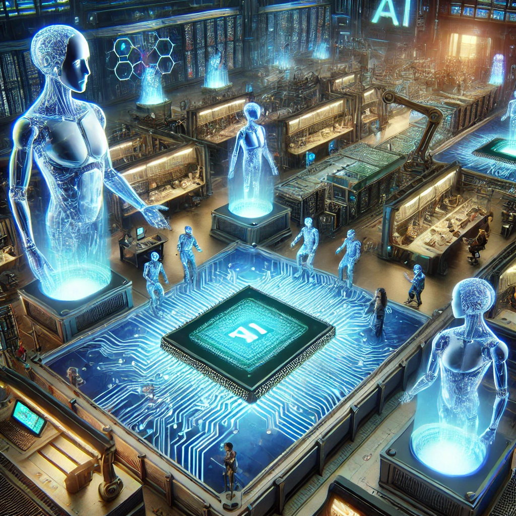
Smarter Chips, Smarter World – The AI-Driven Transformation of the Semiconductor Industry
The world of semiconductor engineering is undergoing a radical transformation, thanks to the integration of artificial intelligence (AI). Chip design, historically considered one of the most intricate and resource-intensive engineering processes, is now being streamlined by AI agents. Companies like Intel, NVIDIA, Google, and IBM are at the forefront of this revolution, leveraging AI-driven methodologies to enhance every phase of chip development, from design to deployment.

The Complexity of Chip Design and the Role of AI
Modern semiconductor development consists of multiple stages, including design, development, testing, validation, and deployment. Each of these phases involves specialized workflows, extensive toolsets, and expert personnel. Traditionally, this process has required painstaking precision and long development cycles. However, AI agents are now stepping in as sophisticated assistants, accelerating tasks such as code generation, simulations, transistor placement, and error detection while maintaining human oversight.
AI’s Role in the Semiconductor Workflow
AI is not replacing engineers; rather, it is augmenting their capabilities. By adopting an “agentic” approach, AI agents are enhancing various aspects of chip development:
- Design Optimization: AI algorithms analyze historical chip designs, suggesting optimal layouts that improve performance, reduce power consumption, and optimize space usage.
- Simulation and Verification: AI-driven simulations enable engineers to test chip designs at scale, identifying potential errors in days rather than weeks. This drastically improves efficiency and reduces costly mistakes before fabrication begins.
- Automation of Routine Tasks: AI agents automate repetitive tasks, freeing up engineers to focus on high-value creative problem-solving.
- EDA (Electronic Design Automation) Enhancement: Companies like Synopsys and Cadence are integrating AI into EDA tools, making chip design smarter and more automated than ever.
How AI Agents Are Trained for Chip Design
Unlike software development, where large language models (LLMs) can be trained on vast repositories of publicly available code, semiconductor engineering is highly proprietary. This presents a unique challenge for AI training. However, industry leaders like Intel, NVIDIA, and Google have an advantage—decades of proprietary data that can be used to train AI models internally.
Rather than developing large models from scratch, companies are leveraging existing AI frameworks such as LangChain, LangGraph, and Google’s DeepMind AI to incorporate domain-specific knowledge and create specialized AI agents. This approach ensures that AI-driven chip design is built upon real-world semiconductor expertise while maintaining data security.
Research and Development Efforts Worldwide
Several organizations and universities are investing heavily in AI-driven chip design:
- Google’s DeepMind: Developed AI models to optimize semiconductor layouts, improving chip performance and reducing design time significantly.
- NVIDIA’s AI-Powered Chip Design: Uses machine learning to enhance GPU and CPU designs, improving efficiency and power optimization.
- IBM’s AI for Semiconductor Manufacturing: Focuses on using AI for photolithography and defect detection to enhance yield and reliability.
- MIT and Stanford Research Labs: Investigating AI algorithms to develop self-learning circuits that continuously optimize their own performance.
- TSMC & Samsung: Integrating AI to improve wafer inspection, defect prediction, and chip fabrication processes.
Current Industry Statistics and Progress
The impact of AI on semiconductor development is already substantial:
- AI-driven design tools are reducing chip design cycles by up to 40%, improving time-to-market.
- Verification and validation times have dropped by 30-50% in companies using AI-assisted simulations.
- AI-optimized chip layouts have improved energy efficiency by 10-20%, as reported by major foundries.
- The global AI in semiconductor market is expected to grow from $1.5 billion in 2023 to $5 billion by 2030.
Practical Applications of AI in Chip Development
AI-Driven Placement and Layout
One of the most critical aspects of chip design is component placement. AI agents analyze historical data and propose optimal layouts, considering factors such as power efficiency, spatial constraints, and signal integrity. Engineers, however, retain the final decision-making authority, ensuring that AI recommendations align with broader design goals.
Automated Verification and Validation
Before fabrication, semiconductor designs must undergo rigorous verification. Traditionally, this process requires weeks of testing. AI agents accelerate verification by identifying design flaws in real time, significantly reducing time-to-market and enhancing product reliability.
AI-Powered Manufacturing and Defect Prediction
AI is being increasingly used in semiconductor fabrication for:
- Wafer inspection: Detecting defects before chips are assembled, improving yield rates.
- Process optimization: AI models predict the best manufacturing parameters for different chip architectures.
- Automated lithography corrections: Adjusting etching patterns in real time to ensure consistency in nanometer-scale circuits.
The Future Vision for AI in Semiconductor Engineering
The integration of AI into chip design is not just a passing trend—it is the future of semiconductor engineering. As AI continues to evolve, we can expect even more sophisticated applications, including:
- Generative AI for Chip Architecture: Future AI models will not only assist in design but also suggest entirely new chip architectures based on performance requirements.
- AI-Powered Fabrication Techniques: AI could revolutionize chip manufacturing by optimizing fabrication techniques, reducing material waste, and improving yield rates.
- Self-Learning AI Models: AI systems that continuously learn from new chip designs will lead to even more advanced automation and predictive capabilities.
- Quantum AI for Semiconductor Research: Leveraging quantum computing to develop next-generation chips with unprecedented efficiency and computational power.
Conclusion: A Paradigm Shift in Engineering
AI is reshaping the way semiconductor chips are designed, verified, and manufactured. Companies like Intel, Google, NVIDIA, and IBM are pioneering the use of AI agents to enhance efficiency, reduce errors, and accelerate product development. While some fear that AI may replace human engineers, the reality is that it is augmenting their capabilities, allowing them to focus on creativity and innovation rather than routine tasks.
As AI technology advances, the semiconductor industry stands on the brink of an unprecedented era of efficiency and innovation. The fusion of human expertise and AI intelligence will drive semiconductor breakthroughs that shape the future of computing, automation, and beyond.
References:
- Intel’s AI-driven chip design initiatives: Intel Newsroom
- AI applications in semiconductor engineering: IEEE Xplore
- Advances in AI for design verification: TechCrunch
- NVIDIA AI-powered chip research: NVIDIA Blog
- Google DeepMind chip layout optimization: DeepMind Research
- MIT & Stanford AI in semiconductor study: MIT Technology Review
AI is not just simplifying chip design—it is redefining it, ushering in an era of smarter, faster, and more efficient semiconductor development.
For more interesting posts, please visit: Blog
-
Слушайте кто ремонт затеял. Фурнитуру ставят дешманскую которая через год клинит. То доставку три месяца ждать. Короче, нашел нормальных производителей — заказать кухню без посредников. Цены ниже рыночных на треть. В общем, смотрите сами по ссылке — заказать кухню заказать кухню Не ведитесь на салоны-прокладки с накруткой. Сам полгода выбирал теперь знаю.
-
Салют, земляки Цены космос а качество мыло То ЛДСП 16 мм а не 18 Короче, реальные ребята с цехом в СПб — кухни СПб напрямую от производителя Фасады из влагостойкого МДФ 19 мм В общем, сохраняйте себе в закладки — глория мебель https://kuhni-spb-wxh.ru Проверяйте производителя по этому списку Сам столько нервов потратил теперь делюсь опытом
-
Ребята кто в Питере Цены задрали как на золото То доставку месяц ждать Короче, реальное производство в Питере — купить кухню в спб от производителя с установкой Замер на следующий день В общем, смотрите сами по ссылке — кухни на заказ от производителя кухни на заказ от производителя Проверяйте производителя по этому списку Сам полгода выбирал теперь знаю
-
Здорова, Питер Объездил полгорода салонов — везде перекупы То ручки отваливаются через месяц Короче, реальное производство в Питере — кухни на заказ по индивидуальным размерам Сделали за три недели как обещали В общем, там цены и каталог работ — кухни под заказ в спб https://kuhni-spb-fpk.ru Не ведитесь на салоны-прокладки с наценкой 100% Сам полгода выбирал теперь знаю
-
Слушайте кто ремонт затеял Замучился я уже кухню искать То кромка кривая через раз Короче, единственные кто делает совестливо — кухни в спб от производителя из массива Фасады на выбор из 50 цветов В общем, сохраняйте в закладки — глория мебель глория мебель Проверяйте производителя по этому списку Сам полгода выбирал теперь знаю
-
Народ всем привет Прошерстил кучу салонов — везде перекупы То сроки по полгода обещают Короче, нашел наконец нормальное производство — кухни СПб от производителя напрямую Сделали за три недели как обещали В общем, там каталог с ценами и реальные отзывы — кухни на заказ спб каталог https://kuhni-spb-uio.ru Проверяйте производителя по этому списку Перешлите тому кто тоже мучается
-
Народ всем привет. На Авито ловить боюсь — нарвусь на брак. То цены такие что проще новую квартиру купить. Короче, нашел наконец нормальное производство — купить кухню от производителя в спб из массива. Цены ниже чем в салонах тысяч на 30-40. В общем, жмите чтобы не потерять контакт — где лучше купить кухню в спб https://zakazat-kuhnyu-rty.ru Проверяйте производителя по этому списку. Перешлите тому кто тоже мучается выбором.
-
online merge online merge
-
Развитая инфраструктура района делает Мосфильмовская Апсайд удобным выбором для людей, которые ценят комфорт и экономию времени на ежедневных поездках – https://mosfilm-upside.ru/
-
Слушайте кто в теме. Фурнитуру ставят дешманскую. Короче, единственные кто не наебывает — заказать кухню без переплат. Гарантия 5 лет. В общем, жмите чтобы не потерять — купить кухню в спб купить кухню в спб Проверяйте производителя. Перешлите тому кто ищет.
-
Ça faisait un moment que je voulais essayer ce site. Télécharger un fichier fiable devenait vraiment galère. J’ai vérifié les dernières mises à jour pour lancer le processus sans erreur. J’ai finalement déniché la bonne source et je voulais vous partager tous les détails, vous pouvez consulter les informations à jour ici: 1xbet download android 1xbet download android. Bref, ce que je voulais vous dire — après l’avoir installée, j’ai été agréablement surpris.
Je n’ai rencontré aucun problème lors du téléchargement. Pour être honnête, c’est la plus stable que j’ai testée — c’est clairement l’application la plus performante du marché. Je vous souhaite plein de réussite et de bons gains…
-
Народ кто в Питере живет. Цены задрали как на золото. То ДСП сыпется. Короче, реальное производство в Питере — заказать кухню без посредников. Проект бесплатно. В общем, сохраняйте — где лучше купить кухню в спб https://zakazat-kuhnyu-qwe.ru Не ведитесь на салоны. Перешлите кому надо.
-
Питерцы отзовитесь. Оббегал все салоны в городе — везде одно и то же. То фасады покоробились от пара. Короче, реальный цех в СПб без наценок — купить кухню от производителя в спб под ключ. Сделали за 2 недели включая замер. В общем, смотрите сами по ссылке — купить заказать кухню купить заказать кухню Проверяйте производителя по этому списку. Перешлите другу кто тоже мучается.
-
The way the post stayed on topic throughout without going on tangents was really refreshing, and a look at actionwithprecision kept that focused approach going, discipline like this in writing is rare and worth recognising because most writers cannot resist wandering off into related subjects that dilute their main point and confuse readers along the way.
-
Благодаря удачному расположению Апсайд Мосфильмовская позволяет быстро добираться до ключевых районов города и одновременно жить в комфортном окружении – новый жк на мосфильмовской
-
Je cherchais une application mobile de qualité pour mes paris. Je n’arrivais pas à mettre la main sur la version officielle. J’ai vérifié les dernières mises à jour pour lancer le processus sans erreur. J’ai finalement trouvé la bonne source et je voulais vous partager tous les détails, vous pouvez consulter les informations à jour ici: xbet apk xbet apk. En deux mots, laissez-moi vous raconter — l’appli tourne super bien sur mon téléphone.
les mises à jour se font toutes seules sans intervention. J’ai comparé plusieurs applis mais celle-ci est la meilleure — croyez-moi, vous ne le regretterez pas, tentez le coup. J’espère que vous serez aussi conquis que moi…
-
Quietly the post solved something I had been turning over without quite knowing how to phrase the question, and a look at claritycreatesmovement extended that quiet solving, content that addresses unformulated needs is content with reader insight and this site has demonstrated that insight at a high rate across the pieces I have read recently.
-
Слушайте кто кухню недавно заказывал Цены космос а качество мыло То фасады кривые Короче, нашел наконец нормальное производство — купить кухню в спб от производителя недорого Фасады из влагостойкого МДФ 19 мм В общем, там каталог с ценами и реальные отзывы — кухни на заказ спб каталог https://kuhni-spb-uio.ru Проверяйте производителя по этому списку Перешлите тому кто тоже мучается
-
J’ai testé plusieurs plateformes sans grand succès. Tout le monde donnait des liens différents, je ne savais plus où aller. Finalement, j’ai pris le temps d’analyser tous les détails techniques. J’ai finalement déniché la bonne source et je voulais vous partager tous les détails, vous pouvez consulter les informations à jour ici: télécharger 1xbet télécharger 1xbet. En deux mots, laissez-moi vous expliquer — l’appli tourne parfaitement bien sur mon téléphone.
l’installation était rapide et simple, pas de tracas. Je vous parle de mon expérience personnelle — c’est clairement l’application la plus performante. J’espère que vous serez aussi satisfaits que moi…
-
ЖК Апсайд Мосфильмовская предлагает комфортные условия для жизни в престижном районе с развитой инфраструктурой и удобным транспортным сообщением: https://mosfilm-upside.ru/
-
Ребята всем привет. То материалы фуфло — картон а не фасады. Объездил уже кучу салонов — тьфу. Короче, нашел наконец нормальный вариант — купить готовую кухню в спб из наличия. И фасады из нормального массива. В общем, вся инфа вот здесь — где купить кухню в спб https://zakazat-kuhnyu-gkl.ru Не ведитесь на салоны-прокладки с наценкой в два раза. Сам полгода мучился теперь делюсь.
-
Слушайте кто недавно кухню делал. В Леруа Мерлен посмотрел — качество ужас. То сроки изготовления по полгода обещают. Короче, нашел наконец нормальное производство — купить кухню от производителя в спб из массива. Цены ниже чем в салонах тысяч на 30-40. В общем, там каталог с ценами и реальные отзывы — купить готовую кухню в спб от производителя https://zakazat-kuhnyu-rty.ru Не ведитесь на салоны в ТЦ которые просто заказывают у тех же китайцев. Перешлите тому кто тоже мучается выбором.
-
online merge online merge
-
Ребята всем привет. Фурнитуру ставят дешманскую. Короче, единственные кто не наебывает — заказать кухню без переплат. Цены ниже на 30%. В общем, смотрите по ссылке — купить кухню в спб от производителя https://zakazat-kuhnyu-bnm.ru Проверяйте производителя. Перешлите тому кто ищет.
-
Ça faisait un moment que je voulais essayer ce site. Je ne trouvais pas la version officielle sur le Play Store. Après avoir suivi les étapes dans le bon ordre, tout a fonctionné. J’ai finalement déniché la bonne source et je voulais vous partager tous les détails, vous pouvez consulter les informations à jour ici: 1xbet apk android 1xbet apk android. Bref, ce que je voulais vous dire — la dernière version est super fluide et intuitive.
les mises à jour se font automatiquement. J’ai comparé plusieurs apps mais celle-ci est la meilleure — ne perdez plus votre temps avec d’autres sites. Je vous souhaite plein de réussite et de bons gains…
-
Район Мосфильмовской давно считается одним из наиболее комфортных для жизни в Москве, а ЖК Апсайд Мосфильмовская органично дополняет преимущества этой локации – https://mosfilm-upside.ru/
-
Народ кто в Питере живет. Обещают одно а по факту другое. То фасады перекошены. Короче, мужики с руками из правильного места — купить готовую кухню в спб с фурнитурой. Замер на следующий день. В общем, вся инфа вот здесь — купить кухню в спб от производителя https://zakazat-kuhnyu-qwe.ru Не ведитесь на салоны. Перешлите кому надо.
-
Питерцы отзовитесь. Оббегал все салоны в городе — везде одно и то же. То фасады покоробились от пара. Короче, реальный цех в СПб без наценок — купить кухню спб в наличии. Сделали за 2 недели включая замер. В общем, вся инфа вот тут — купить кухню производителя в спб купить кухню производителя в спб Не ведитесь на салоны-прокладки с накруткой. Перешлите другу кто тоже мучается.
-
Качественная архитектура, удобные планировки и развитая инфраструктура делают ЖК Апсайд Мосфильмовская привлекательным для самых разных категорий покупателей: апсайд мосфильмовская официальный сайт
-
Вот решил поделиться информацией — какой способ действительно работает для международных транзакций. Вот здесь всё по полочкам расписано: оплата через посредника за рубеж https://mezhdunarodnye-platezhi-fra.ru Основной вывод, который я сделал — разница в итоговой сумме бывает значительной. Стоит учитывать, что любой международный перевод — имеет свои нюансы в зависимости от выбранного способа. И ещё один момент — прежде чем отправлять средства стоит проверить итоговую сумму. Без этого можно получить менее выгодные условия. Резюмируя — необходимо проверять информацию перед любой отправкой средств.
-
Solid value for anyone willing to read carefully, and a look at yundizhi02 extends that value across the rest of the site, this is the kind of place that rewards return visits rather than offering everything in a single splashy post and then leaving readers nothing to come back for later which is unfortunately common.
-
Кровь и пламя возвращаются на экраны – дом дракона 3 сезон новые спойлеры 2026. Раскол королевства достиг точки невозврата – Рейнира и Эйгон ведут своих драконов в решающие схватки. Древние пророчества сбываются, родная кровь становится врагом, а трон требует новых жертв. Долгожданное продолжение саги!
-
Je cherchais une application mobile de qualité pour mes paris. Tout le monde donnait des liens différents, impossible de s’y retrouver. Finalement, j’ai pris le temps d’analyser tous les détails techniques. J’ai finalement trouvé la bonne source et je voulais vous partager tous les détails, vous pouvez consulter les informations à jour ici: telecharger 1xbet sur iphone telecharger 1xbet sur iphone. Voilà, pour être clair net et précis — la dernière version est hyper fluide et agréable à utiliser.
Je n’ai eu aucun problème lors du téléchargement. Pour être franc, c’est la plus fiable que j’aie testée — c’est sans doute l’application la plus performante du marché. J’espère que vous serez aussi conquis que moi…
-
Ça faisait un moment que je voulais tester cette plateforme. Je ne trouvais pas la version officielle sur le Play Store. Après avoir suivi les étapes dans le bon ordre, tout a fonctionné. J’ai finalement déniché la bonne source et je voulais vous partager tous les détails, vous pouvez consulter les informations à jour ici: 1xbet ci apk 1xbet ci apk. Bref, ce que je voulais vous dire — la dernière version est super fluide et intuitive.
l’installation était rapide et sans complication. Pour être honnête, c’est la plus stable que j’ai testée — croyez-moi, vous ne serez pas déçus, essayez-la sans hésiter. J’espère que vous serez aussi satisfaits que moi…
-
J’ai testé plusieurs plateformes sans grand succès. Télécharger un fichier sûr devenait un vrai parcours du combattant. Après avoir suivi les étapes dans le bon ordre, tout a fonctionné. J’ai finalement déniché la bonne source et je voulais vous partager tous les détails, vous pouvez consulter les informations à jour ici: 1xbet 1xbet. Voilà, pour être clair avec vous — après l’avoir installée, j’ai été vraiment surpris.
l’installation était rapide et simple, pas de tracas. J’ai comparé plusieurs apps mais celle-ci est la meilleure — ne perdez plus votre temps avec d’autres sites. J’espère que vous serez aussi satisfaits que moi…
-
Lalabet Casino lalabet exclusieve bonussen is een snel en modern online casino waar je direct kunt spelen zonder gedoe. Kies uit populaire slots en live games en profiteer van aantrekkelijke bonussen voor nieuwe spelers. Start nu, activeer je bonus en ontdek hoeveel je kunt winnen — speel meteen en mis geen kansen op winst!
-
Ребята всем привет. Фурнитуру ставят дешманскую. Короче, нашел нормальный вариант — купить кухню от производителя в спб. Фасады из массива. В общем, смотрите по ссылке — купить готовую кухню от производителя https://zakazat-kuhnyu-bnm.ru Не ведитесь на салоны. Перешлите тому кто ищет.
-
http://bbs.sdhuifa.com/home.php?mod=space&uid=1150378 Занимаемся арендой авто в Краснодаре без залога и ограничения по пробегу с подачей в аэропорт и жд вокзал
-
Ребята кто в Питере живет. Задолбался я уже два месяца мучиться. То материал эконом — покоробится через месяц. Короче, нашел наконец нормальное производство — купить кухню от производителя в спб из массива. Кромка на немецком оборудовании. В общем, смотрите сами по ссылке — купить готовую кухню от производителя https://zakazat-kuhnyu-rty.ru Не ведитесь на салоны в ТЦ которые просто заказывают у тех же китайцев. Сам столько нервов потратил теперь делюсь.
-
Питерцы отзовитесь. Вечно то цены конские у дилеров. Пересмотрел ютуб с отзывами — голова пухнет. Короче, единственные кто не наебывает — купить готовую кухню в спб из наличия. И фасады из нормального массива. В общем, там каталог и цены и отзывы реальные — купить кухню в спб купить кухню в спб Не ведитесь на салоны-прокладки с наценкой в два раза. Сам полгода мучился теперь делюсь.
-
merge games merge games
-
Прокат яхт Сириус предлагает широкий выбор судов для различных форматов отдыха. Можно подобрать яхту как для небольшой компании, так и для крупного мероприятия: https://yachtkater.ru/
-
Je cherchais une bonne appli mobile pour mes paris sportifs. Télécharger un fichier fiable devenait vraiment galère. J’ai vérifié les dernières mises à jour pour lancer le processus sans erreur. J’ai finalement déniché la bonne source et je voulais vous partager tous les détails, vous pouvez consulter les informations à jour ici: 1xbet apk 2026 télécharger gratuitement 1xbet apk 2026 télécharger gratuitement. Bref, ce que je voulais vous dire — après l’avoir installée, j’ai été agréablement surpris.
Je n’ai rencontré aucun problème lors du téléchargement. J’ai comparé plusieurs apps mais celle-ci est la meilleure — ne perdez plus votre temps avec d’autres sites. J’espère que vous serez aussi satisfaits que moi…
-
Lalabet Casino lalabet revieuw is een snel en modern online casino waar je direct kunt spelen zonder gedoe. Kies uit populaire slots en live games en profiteer van aantrekkelijke bonussen voor nieuwe spelers. Start nu, activeer je bonus en ontdek hoeveel je kunt winnen — speel meteen en mis geen kansen op winst!
-
Lalabet Casino lalabet casino review is een snel en modern online casino waar je direct kunt spelen zonder gedoe. Kies uit populaire slots en live games en profiteer van aantrekkelijke bonussen voor nieuwe spelers. Start nu, activeer je bonus en ontdek hoeveel je kunt winnen — speel meteen en mis geen kansen op winst!
-
Thanks for the breakdown, it gave me a clearer picture of something I had been confused about for a while now, and a stop at apiculatea closed the remaining gaps in my understanding nicely, no need to hunt around twenty other articles to put the pieces together which is a real time saver.
-
Решил проблему только когда наткнулся — какой сервис не сдирает три шкуры для международных переводов. Случайно набрел на годный материал: международные транзакции международные транзакции Суть вот в чём — курс конвертации часто занижают. Согласитесь, абсурд любой очередной международный перевод — это головная боль с отслеживанием статуса. И да, кстати — прежде чем отправлять деньги обязательно сверьте итоговую сумму. Иначе легко попасть на лишние траты. Как итог — лучше один раз изучить тему перед любой отправкой.
-
Кровь и пламя возвращаются на экраны – дом дракона смотреть 3 сезон дата. Раскол королевства достиг точки невозврата – Рейнира и Эйгон ведут своих драконов в решающие схватки. Древние пророчества сбываются, родная кровь становится врагом, а трон требует новых жертв. Долгожданное продолжение саги!
-
демонтаж санузла цена Наши расценки на демонтажные работы являются одними из самых конкурентных в городе. Мы предлагаем прозрачное ценообразование и качественный сервис.
-
Je cherchais une application fiable pour mon téléphone. Télécharger un fichier sûr était devenu un vrai casse-tête. Après avoir suivi les étapes dans le bon ordre, tout a fonctionné. J’ai finalement trouvé la bonne source et je voulais vous partager tous les détails, vous pouvez consulter les informations à jour ici: 1xbet apk android 1xbet apk android. En résumé, laissez-moi vous expliquer — après l’avoir installée sur mon téléphone, j’ai été agréablement surpris.
Je n’ai rencontré aucun problème lors du téléchargement. Pour être honnête, c’est la plus fiable que j’ai trouvée — ne perdez plus votre temps ailleurs. Bon courage à tous…
-
https://jobs.tdwi.org/employers/4207597-1xbet-promo-code-free-spins-1xbonus130-130-spins Занимаемся арендой авто в Краснодаре без залога и ограничения по пробегу с подачей в аэропорт и жд вокзал
-
Прокат яхт в Адлере позволяет организовать незабываемый отдых для семьи, друзей или коллег. Прогулка по морю подарит яркие эмоции и красивые фотографии: аренда катера Сириус
-
Je cherchais une application mobile de qualité pour mes paris. Télécharger un fichier sûr devenait un vrai casse-tête chinois. J’ai vérifié les dernières mises à jour pour lancer le processus sans erreur. J’ai finalement trouvé la bonne source et je voulais vous partager tous les détails, vous pouvez consulter les informations à jour ici: 1x bet apk 1x bet apk. Voilà, pour être clair net et précis — l’appli tourne super bien sur mon téléphone.
Je n’ai eu aucun problème lors du téléchargement. Je vous fais part de mon retour d’expérience — croyez-moi, vous ne le regretterez pas, tentez le coup. J’espère que vous serez aussi conquis que moi…
-
Ça faisait un moment que je voulais tester cette plateforme. Tout le monde recommandait des adresses différentes, dur de s’y retrouver. Après avoir suivi les étapes dans le bon ordre, tout a fonctionné. J’ai finalement déniché la bonne source et je voulais vous partager tous les détails, vous pouvez consulter les informations à jour ici: 1xbet.apk http://www.countryontheriver.com. En deux mots, laissez-moi vous expliquer — l’appli tourne parfaitement sur mon smartphone.
l’installation était rapide et sans complication. Pour être honnête, c’est la plus stable que j’ai testée — c’est clairement l’application la plus performante du marché. Je vous souhaite plein de réussite et de bons gains…
-
Нашёл интересный материал по этому вопросу — где предлагают адекватные условия для международных платежей. Нашёл подробный анализ ситуации: онлайн перевод денег за границу https://mezhdunarodnye-platezhi-fra.ru Суть в следующем — разница в итоговой сумме бывает значительной. Стоит учитывать, что любой перевод за границу онлайн — связан с разными типами комиссий. Дополнительная информация — до проведения операции рекомендуется сравнить несколько вариантов. Без этого можно получить менее выгодные условия. В итоге — стоит потратить время на анализ перед любой отправкой средств.
-
Je cherchais une application mobile fiable pour mes paris. Télécharger un fichier sûr devenait un vrai parcours du combattant. Finalement, j’ai pris le temps d’analyser tous les détails techniques. J’ai finalement déniché la bonne source et je voulais vous partager tous les détails, vous pouvez consulter les informations à jour ici: 1xbet app 1xbet app. En deux mots, laissez-moi vous expliquer — après l’avoir installée, j’ai été vraiment surpris.
les mises à jour se font automatiquement sans intervention. Je vous parle de mon expérience personnelle — c’est clairement l’application la plus performante. J’espère que vous serez aussi satisfaits que moi…
-
A piece that ended with a clean landing rather than fading out, and a look at kaitori-gk maintained the same crisp conclusions, endings that resolve rather than dissolve are a sign of careful structural thinking and this site has clearly invested in how its pieces conclude rather than letting them simply run out of energy.
-
Кровь и пламя возвращаются на экраны – https://dom-drakona-3.top/. Раскол королевства достиг точки невозврата – Рейнира и Эйгон ведут своих драконов в решающие схватки. Древние пророчества сбываются, родная кровь становится врагом, а трон требует новых жертв. Долгожданное продолжение саги!
-
Прокат яхт в Сириусе позволяет организовать отдых премиального уровня без необходимости владеть собственным судном. Гости могут наслаждаться просторными палубами, красивыми морскими видами и атмосферой настоящего путешествия. Такой формат отдыха подходит как для коротких прогулок, так и для длительного пребывания на воде, когда хочется полностью погрузиться в атмосферу моря – https://yachtkater.ru/
-
демонтаж сантехкабины в панельном доме Точный демонтаж фундамента цена которого зависит от типа бетона и глубины залегания, лучше доверять профессионалам. Мы используем спецтехнику для быстрого сноса.
-
Lalabet Casino lalabet bijvullen is een snel en modern online casino waar je direct kunt spelen zonder gedoe. Kies uit populaire slots en live games en profiteer van aantrekkelijke bonussen voor nieuwe spelers. Start nu, activeer je bonus en ontdek hoeveel je kunt winnen — speel meteen en mis geen kansen op winst!
-
Кровь и пламя возвращаются на экраны – https://dom-drakona-3.top/. Раскол королевства достиг точки невозврата – Рейнира и Эйгон ведут своих драконов в решающие схватки. Древние пророчества сбываются, родная кровь становится врагом, а трон требует новых жертв. Долгожданное продолжение саги!
-
Если вы хотите провести отпуск ярко и получить новые впечатления, стоит арендовать яхту в Адлере. Во время прогулки можно увидеть самые красивые участки побережья, сделать эффектные фотографии и насладиться спокойной атмосферой открытого моря. Многие выбирают яхтенные прогулки для особых событий, ведь отдых на воде создает неповторимое настроение и дарит множество положительных эмоций – https://yachtkater.ru/
-
Кровь и пламя возвращаются на экраны – сериал дом дракона 3 сезон смотреть онлайн. Раскол королевства достиг точки невозврата – Рейнира и Эйгон ведут своих драконов в решающие схватки. Древние пророчества сбываются, родная кровь становится врагом, а трон требует новых жертв. Долгожданное продолжение саги!
-
https://cc-msk.ru/user/sharapowak Занимаемся арендой авто в Краснодаре без залога и ограничения по пробегу с подачей в аэропорт и жд вокзал
-
Lalabet Casino lalabet illegaal is een snel en modern online casino waar je direct kunt spelen zonder gedoe. Kies uit populaire slots en live games en profiteer van aantrekkelijke bonussen voor nieuwe spelers. Start nu, activeer je bonus en ontdek hoeveel je kunt winnen — speel meteen en mis geen kansen op winst!
-
Честно, задолбался искать нормальный вариант — как выбрать реально работающий способ для международных платежей. Случайно набрел на годный материал: перевод денежных средств за границу перевод денежных средств за границу Самое главное, что я вынес — скрытые платежи всплывают в последний момент. Согласитесь, абсурд любой очередной международный перевод — это головная боль с отслеживанием статуса. И да, кстати — прежде чем отправлять деньги сравните эффективный курс. Без этого легко остаться в минусе только на конвертации. Моё мнение — лучше один раз изучить тему перед любой отправкой.
-
Felt this in a way I cannot quite explain, the topic just hit different here, and a stop at onkm continued in that vein, sometimes you find a site whose perspective lines up with how you have been thinking and reading their work feels like a small relief which I appreciated more than I expected.
-
демонтаж дома из бруса цена Профессиональный снос построек на участке — это гарантия безопасности и быстрого освобождения территории. Мы берем на себя все заботы по вывозу строительного лома.
-
Аренда яхт Сириус позволяет почувствовать себя настоящим участником морского путешествия. Комфортные условия на борту делают отдых максимально приятным и расслабляющим: https://yachtkater.ru/
-
Нашёл интересный материал по этому вопросу — какой способ действительно работает для платежей за рубежом. Товарищ скинул ссылку на качественный разбор: агент по международным платежам https://mezhdunarodnye-platezhi-fra.ru Основной вывод, который я сделал — не все сервисы одинаково прозрачны. Дело в том, что любой трансграничный платёж — требует предварительного сравнения условий. Дополнительная информация — прежде чем отправлять средства стоит проверить итоговую сумму. Без этого можно столкнуться с неожиданными расходами. Резюмируя — лучше заранее разобраться в вопросе перед любой отправкой средств.
-
Vox Casino vox casino kod bez depozytu to nowoczesna platforma dla miłośników gier kasynowych online. Gracze mogą korzystać z szerokiego wyboru automatów, gier stołowych oraz atrakcyjnych promocji przygotowanych zarówno dla nowych, jak i stałych użytkowników. Dodatkowe korzyści zapewniają kody promocyjne, darmowe spiny oraz bonusy bez depozytu dostępne w wybranych ofertach.
-
Vox Casino vox casino kod promocyjny 2026 bez depozytu to nowoczesna platforma dla miłośników gier kasynowych online. Gracze mogą korzystać z szerokiego wyboru automatów, gier stołowych oraz atrakcyjnych promocji przygotowanych zarówno dla nowych, jak i stałych użytkowników. Dodatkowe korzyści zapewniają kody promocyjne, darmowe spiny oraz bonusy bez depozytu dostępne w wybranych ofertach.
-
Vox Casino kod do vox casino to nowoczesna platforma dla miłośników gier kasynowych online. Gracze mogą korzystać z szerokiego wyboru automatów, gier stołowych oraz atrakcyjnych promocji przygotowanych zarówno dla nowych, jak i stałych użytkowników. Dodatkowe korzyści zapewniają kody promocyjne, darmowe spiny oraz bonusy bez depozytu dostępne w wybranych ofertach.
-
Je cherchais une application fiable pour mon téléphone. Je n’arrivais pas à trouver la bonne version sur le Play Store. Après avoir suivi les étapes dans le bon ordre, tout a fonctionné. J’ai finalement trouvé la bonne source et je voulais vous partager tous les détails, vous pouvez consulter les informations à jour ici: télécharger 1xbet pour android télécharger 1xbet pour android. Bref, ce que je voulais dire — la dernière version est vraiment bien conçue.
les mises à jour se font automatiquement. Je vous parle de mon expérience personnelle — ne perdez plus votre temps ailleurs. Bon courage à tous…
-
Честно говоря, — какой сервис выбрать для международных платежей. В одном блоге вычитал вот этот обзор: перевод за границу онлайн перевод за границу онлайн Если коротко, — не все способы одинаково выгодны. Потому что очередной международный перевод — это всегда стресс. И ещё момент, — перед тем как отправлять проверьте несколько вариантов. Иначе легко попасть на лишние траты. Резюмируя, — стоит разобраться заранее.
-
Долго не мог понять, в чем подвох — какой сервис не сдирает три шкуры для международных транзакций. В одном обсуждении попался дельный совет: онлайн перевод денег за границу онлайн перевод денег за границу Самое главное, что я вынес — банковские комиссии могут быть грабительскими. Ну сами подумайте любой перевод за границу онлайн — это головная боль с отслеживанием статуса. Вот ещё важный момент — до любой операции с валютой обязательно сверьте итоговую сумму. Иначе легко остаться в минусе только на конвертации. Моё мнение — лучше один раз изучить тему перед любой отправкой.
-
Наболело уже, честно говоря — как нормально отправлять деньги для международных платежей. Порылся в интернете — смотрите, тут годнота: платежный агент за рубежом https://mezhdunarodnye-platezhi-tov.ru Короче, суть такая — есть реальные подводные камни. Потому что любой перевод за границу онлайн — это лотерея с банковскими процентами. И да, кстати — перед финальным кликом проверьте актуальные отзывы. В противном случае легко остаться в минусе. Моё мнение — лучше сначала изучить тему.
-
частный коррекционный детский сад в москве Наш детский коррекционный сад в Москве помогает детям преодолевать трудности в развитии через игру и общение. Мы гордимся тем, что наши выпускники уверенно входят в мир школьного обучения.
-
Vox Casino czy vox casino jest wyplacalne to nowoczesna platforma dla miłośników gier kasynowych online. Gracze mogą korzystać z szerokiego wyboru automatów, gier stołowych oraz atrakcyjnych promocji przygotowanych zarówno dla nowych, jak i stałych użytkowników. Dodatkowe korzyści zapewniają kody promocyjne, darmowe spiny oraz bonusy bez depozytu dostępne w wybranych ofertach.
-
частный коррекционный детский сад в москве Коррекционный детский сад «Нейроангел» в Москве — это место, где вера в возможности каждого ребенка становится фундаментом нашей работы. Мы помогаем детям раскрыться и стать уверенными в себе.
-
Новости Читайте ключевые Новости России и мира в одной ленте, чтобы иметь полное представление о глобальной повестке дня. Мы анализируем влияние международных событий на жизнь внутри страны.
-
Новости в России As a dedicated News Agency, we provide round-the-clock updates to keep you informed during times of change. Your trust is our greatest asset.
-
Нашёл интересный материал по этому вопросу — как правильно организовать процесс для платежей за рубежом. Товарищ скинул ссылку на качественный разбор: прием оплаты из-за рубежа https://mezhdunarodnye-platezhi-fra.ru Основной вывод, который я сделал — не все сервисы одинаково прозрачны. Дело в том, что любой международный перевод — требует предварительного сравнения условий. Также стоит отметить — прежде чем отправлять средства имеет смысл изучить актуальные тарифы. Без этого можно получить менее выгодные условия. В итоге — лучше заранее разобраться в вопросе перед любой отправкой средств.
-
частный коррекционный детский сад в москве Наш детский коррекционный сад в Москве предоставляет профессиональную помощь в комфортных для ребенка условиях. Мы работаем по индивидуальным маршрутам, которые строятся исходя из потребностей каждого.
-
Vox Casino kody na vox casino to nowoczesna platforma dla miłośników gier kasynowych online. Gracze mogą korzystać z szerokiego wyboru automatów, gier stołowych oraz atrakcyjnych promocji przygotowanych zarówno dla nowych, jak i stałych użytkowników. Dodatkowe korzyści zapewniają kody promocyjne, darmowe spiny oraz bonusy bez depozytu dostępne w wybranych ofertach.
-
коррекционный детский сад нейроангел в москве Частный коррекционный детский сад в Москве обеспечивает индивидуальное внимание к каждому ребенку в течение всего дня. Наши специалисты знают, как найти подход даже к самым непростым ситуациям.
-
Ça fait longtemps que je voulais tester cette plateforme. Télécharger un fichier sûr était devenu un vrai casse-tête. J’ai vérifié les dernières mises à jour pour lancer le processus sans erreur. J’ai finalement trouvé la bonne source et je voulais vous partager tous les détails, vous pouvez consulter les informations à jour ici: 1xbet app download 1xbet app download. En résumé, laissez-moi vous expliquer — l’application mobile fonctionne parfaitement bien.
l’installation était simple et rapide, pas de souci à vous faire. Pour être honnête, c’est la plus fiable que j’ai trouvée — croyez-moi, vous ne serez pas déçus, essayez-la. J’espère que vous serez aussi satisfaits que moi…
-
Долго не мог понять, в чем подвох — где условия адекватные, а не грабёж для платежей за рубежом. Случайно набрел на годный материал: онлайн перевод денег за границу онлайн перевод денег за границу Самое главное, что я вынес — не все способы одинаково прозрачны. Потому что любой перевод за границу онлайн — это реальная финансовая лотерея. Обратите внимание, многие не в курсе — перед финальным подтверждением проверьте все комиссии до копейки. В противном случае легко потерять приличную сумму. Моё мнение — стоит разобраться заранее перед любой отправкой.
-
Знаете, — как найти адекватный способ перевода денег за границу онлайн. В одном блоге вычитал вот этот обзор: переводы денег за границу https://mezhdunarodnye-platezhi-nar.ru Если коротко, — комиссии могут сильно отличаться. Да и сами понимаете очередной международный перевод — это лотерея с банковскими комиссиями. Обратите внимание — до любой операции проверьте несколько вариантов. Без этого легко попасть на лишние траты. Резюмируя, — стоит разобраться заранее.
-
types of monopoly in economics https://monopolyy.live/
-
monopoly big bola result https://monopolyy.live/
-
monopoly big baller bonus https://monopolyy.live/
-
play monopoly live https://monopolyy.live/
-
Главные новости Интересные Новости в России и мире всегда доступны на нашем сайте в удобном формате для чтения с любых устройств. Мы следим за развитием технологий.
-
В общем, решил поделиться — какой вариант реально рабочий для международных переводов. На одном форуме вычитал — смотрите, тут годнота: международные платежи https://mezhdunarodnye-platezhi-tov.ru Если по делу, то — комиссии у всех разные как с неба. Потому что любой перевод за границу онлайн — это всегда головная боль без нормальной инфы. Обратите внимание — до любой операции посчитайте итоговую сумму с комиссиями. Иначе легко попасть на лишние траты. Моё мнение — лучше сначала изучить тему.
-
Новости в России и мире Узнавайте важные Новости, которые формируют будущее, на страницах нашего электронного издания. Мы делаем информацию доступной и понятной для каждого жителя страны.
-
Хороший дизайн офиса снижает риск ошибок на стройке, потому что заранее показывает, где будут оборудование, мебель, свет, коммуникации и ключевые зоны. Это помогает подрядчикам работать точнее, а владельцу контролировать результат https://dzen.ru/a/aiiAirDNJ2dJt-hJ
-
детский коррекционный сад в москве Коррекционный детский сад «Нейроангел» в Москве — это надежный помощник в вопросах воспитания и коррекции развития. Наши эксперты всегда готовы поддержать и направить вашего ребенка.
-
Кстати, недавно наткнулся на обсуждение актуальной темы. Сам уже давно ищу нормальный способ совершить платеж, без лишних проблем и комиссий. В общем, если вас тоже затрагивают эти вопросы — взгляните тут. Реальные примеры и подводные камни по переводу за границу онлайн: перевод за границу онлайн перевод за границу онлайн И да, имейте в виду, что без нормального обменного курса любые трансграничные переводы превращаются в сплошной геморрой. Добавлю по опыту — всегда смотрите несколько сервисов, прежде чем платить.
-
коррекционный детский сад нейроангел в москве Ищете профессиональный детский коррекционный сад в Москве для всестороннего развития вашего ребенка? Наши специалисты используют передовые методики, чтобы помочь детям адаптироваться и раскрыть свой потенциал в комфортной среде.
-
Новости России и мира Наши Новости в России и мире охватывают широкий спектр тем: от геополитики до инноваций в технологиях. Будьте в центре событий и понимайте суть происходящего благодаря нашим экспертным обзорам.
-
Дизайн фитнес-клуба должен работать не только на визуальное впечатление, но и на экономику проекта. Когда заранее продуманы планировка, свет, материалы и маршруты людей, пространство проще запустить, обслуживать и развивать без лишних переделок https://dzen.ru/a/aih7yu5wim_beO7J
-
Вот решил поделиться информацией — как правильно организовать процесс для международных платежей. В одном обсуждении попался дельный обзор: онлайн перевод денег за границу https://mezhdunarodnye-platezhi-fra.ru Основной вывод, который я сделал — курс конвертации может существенно отличаться. Дело в том, что любой трансграничный платёж — имеет свои нюансы в зависимости от выбранного способа. И ещё один момент — перед подтверждением перевода стоит проверить итоговую сумму. Без этого можно получить менее выгодные условия. В итоге — лучше заранее разобраться в вопросе перед любой отправкой средств.
-
I’ve got the horror stories to back that up. You see this amazing deal online — shiny Audi, unlimited miles, price that makes you want to book right now. Plus they put a $5000 hold on your card and say “don’t worry about it”. Fool me nineteen times? That’s just Miami being Miami. luxury car rental in miami. anyone who’s taken the bus here knows what I mean. leather seats that won’t melt your skin in August. most are shiny garbage with fake five-star reviews. Finally found one outfit that actually delivers. Here’s the only honest source for premium rides across South Florida
rent a urus for a day https://luxury-car-rental-miami-19.com Yeah parking in Brickell will cost you — but that’s life here. drive safe and skip that “tire protection” upsell — total waste. -
Свежие новости Мы — современное Новостное агентство, использующее новейшие способы подачи информации для своих пользователей. Получайте важные оповещения прямо на свой смартфон.
-
Решил проблему только когда наткнулся — как выбрать реально работающий способ для платежей за рубежом. Товарищ скинул ссылку на нормальный разбор: переводы за рубеж переводы за рубеж Короче, если по факту — курс конвертации часто занижают. Потому что любой подобный трансграничный платёж — это реальная финансовая лотерея. Обратите внимание, многие не в курсе — до любой операции с валютой проверьте все комиссии до копейки. Иначе легко остаться в минусе только на конвертации. Моё мнение — не ленитесь проверять информацию перед любой отправкой.
-
Наболело уже, честно говоря — как нормально отправлять деньги для международных переводов. Порылся в интернете — держите, вот нормальный разбор: оплата за границу оплата за границу Короче, суть такая — курс валют может убить любую выгоду. Ну сами понимаете любой подобный?? перевод — это лотерея с банковскими процентами. Вот ещё какой момент — прежде чем отправлять посчитайте итоговую сумму с комиссиями. Без этого легко остаться в минусе. Короче — не поленитесь проверить информацию перед отправкой.
-
Вот уже несколько недель мучаюсь с этим вопросом — какой сервис выбрать для международных платежей. В одном блоге вычитал вот этот обзор: отправка денег за рубеж https://mezhdunarodnye-platezhi-nar.ru Если коротко, — комиссии могут сильно отличаться. Да и сами понимаете очередной международный перевод — это потеря времени без нормальной инфы. И ещё момент, — прежде чем платить сравните условия. В противном случае легко пролететь с курсом. Короче, — не поленитесь проверить информацию.
-
частный коррекционный детский сад в москве В нашем частном коррекционном детском саду в Москве каждый ребенок получает шанс на полноценную социализацию. Мы активно работаем с родителями для достижения наилучших результатов в развитии детей.
-
Alright, last one I swear — but someone’s gotta warn people about this Miami rental mess. You spot this killer offer online — brand new Porsche, zero excess, price that screams “book me”. Different car waiting — dents everywhere, smells like cheap air freshener covering something worse, and that “killer price”? Doesn’t include the mandatory $55 daily toll pass or the $450 “convenience fee” they invent at checkout. Twenty years in South Florida and these clowns still almost get me. luxury car for rent. Miami without real wheels is basically a disaster. South Beach dinner, Design District shopping, or a spontaneous Keys adventure — AC must be arctic and unlimited miles non-negotiable. most are shiny garbage with fake five-star reviews from God knows where. no games, no bait-and-switch, no hidden fees on page 8. prices change hourly so don’t wait around:
exotic car rental south beach miami exotic car rental south beach miami Yeah parking in South Beach will cost you a nice bottle of wine — but that’s the Miami tax. drive safe and absolutely skip that “windshield protection” upsell — pure profit for them, zero for you. -
детский коррекционный сад в москве Частный коррекционный детский сад в Москве предлагает комфортную среду для ежедневного пребывания и развития детей. Мы уделяем максимум времени развитию коммуникативных способностей каждого малыша.
-
Irwin Casino ir win bietet eine moderne Plattform für Fans von Online-Casinospielen. Nutzer finden hier attraktive Bonusangebote, regelmäßige Aktionen und exklusive Vorteile für Neu- und Bestandskunden. Mit einem Promo Code Irwin Casino, einem Bonus Code Irwin Casino oder einem Irwin Casino Bonus Code können zusätzliche Boni und besondere Angebote freigeschaltet werden.
-
Wer nach einem zuverlässigen Online-Casino sucht, findet bei Irwin Casino irwin casino promo code no deposit bonus eine große Auswahl an Spielen und attraktiven Promotionen. Regelmäßige Bonusaktionen, exklusive Angebote und spezielle Belohnungen sorgen für zusätzlichen Spielspaß. Mit einem Irwin Casino Promo Code oder einem aktuellen Bonus Code lassen sich weitere Vorteile und interessante Prämien sichern.
-
Главные новости Working as a global News Agency, we provide professional reports from every corner of the planet. We connect people with reliable stories that matter.
-
Кстати, недавно наткнулся на обсуждение текущей ситуации с переводами. Сам уже не первый месяц ищу нормальный способ провести транзакцию, без лишних проблем и комиссий. В общем, если вас тоже волнует эта тема — узнайте подробности тут. Реальные примеры и подводные камни по международным платежам: перевод платежей за границу перевод платежей за границу И ещё момент имейте в виду, что без прозрачных комиссий любые международные платежи превращаются в головную боль. Ну и напоследок — всегда смотрите несколько сервисов, прежде чем платить.
-
Irwin Casino irwin casino de bietet eine moderne Plattform für Fans von Online-Casinospielen. Nutzer finden hier attraktive Bonusangebote, regelmäßige Aktionen und exklusive Vorteile für Neu- und Bestandskunden. Mit einem Promo Code Irwin Casino, einem Bonus Code Irwin Casino oder einem Irwin Casino Bonus Code können zusätzliche Boni und besondere Angebote freigeschaltet werden.
-
I’ve stepped on enough landmines to write a guidebook. You find this tempting offer online — gorgeous convertible, fair daily rate, looks like a steal. Completely different car waiting — bald tires, smell like someone lived in it, and that “fair rate”? Doesn’t include the mandatory $45 daily toll pass or the $350 “location fee” they spring on you. Fool me eighteen times? That’s just the 305 way of life. luxury car rental miami florida. anyone who’s tried the trolley knows the struggle. leather seats that won’t brand your legs in July. I’ve tested so many rental companies I’ve honestly lost count. Finally found one outfit that doesn’t play games. Here’s the only honest source for premium rides across South Florida
porsche for rent near me https://luxury-car-rental-miami-18.com Yeah parking in Wynwood will cost you — but that’s Miami for you. Anyway glad there’s at least one honest operator left. -
I’ve been burned more times than a cheap steak at a tourist trap. You find this amazing offer online — beautiful car, great rate, everything seems perfect. Completely different car waiting for you — smells like stale cigarettes, check engine light glowing, and that “great rate”? Doesn’t include the mandatory $35 daily toll pass, the $200 cleaning fee, or the $75 “after-hours pickup” charge. Sixteen years in Miami and these tricks still pop up like bad weeds. luxury car rental miami florida. Miami without real wheels is basically a slow death. Design District shopping, late-night South Beach cruising, or a spontaneous Keys trip — AC must be freezing and unlimited miles or walk. most are just pretty websites hiding the same old garbage. no tricks, no switch, no surprise fees. Here’s the only honest place for premium rentals across South Florida
escalade for rent near me escalade for rent near me Yeah parking in Miami Beach will cost you — but that’s life here. Anyway glad someone’s still honest in this business. -
Okay folks gather round — another Miami rental horror story coming at you. You see this killer deal online — brand new Mercedes, unlimited miles, price that makes you want to book immediately. Completely different car sitting there — scratches everywhere, smells like someone hotboxed it for a week, and that “killer price”? Doesn’t include the mandatory $45 daily insurance or the $400 “destination fee” they add at the very end. Thirteen years in South Florida and these clowns still almost get me. When you’re hunting for a legit luxury car rental miami. anyone who’s taken the Metro here knows the struggle is real. leather seats that won’t fuse to your skin in the August heat. most are polished garbage with fake five-star reviews bought from some shady service. no games, no bait-and-switch, no hidden fees buried on page 4 of the contract. Here’s the only straight shooter for premium rides across South Florida
luxury cars to rent near me https://luxury-car-rental-miami-13.com also bring polarized shades unless you enjoy driving into the sun like a blind bat every evening. drive safe and definitely skip that “tire protection” upsell — pure robbery. -
Russian News Agency Актуальные Новости РФ — это ваш инструмент для отслеживания социально-экономических изменений в стране. Мы предоставляем данные в максимально простом виде.
-
коррекционный детский сад нейроангел в москве В частном коррекционном детском саду в Москве ваш ребенок будет в надежных руках профессионалов. Мы создаем условия для развития навыков, необходимых каждому ребенку для адаптации в мире.
-
I’ve seen it all, and most of it isn’t pretty. Then you actually go to pick it up. Different car sitting there — dents you didn’t see, AC that barely works, and that “reasonable rate”? Doesn’t include the mandatory $40 daily insurance or the $300 “processing fee” they add at the last second. Seventeen years in South Florida and these scams still pop up. luxury car rental in miami. Miami without good wheels is basically a headache. Coconut Grove dinner, Bal Harbour shopping, or a spontaneous drive to the Keys — AC must be cold and unlimited miles or forget it. I’ve tried so many rental places I’ve lost count. no games, no hidden fees, no nonsense. Here’s the only honest spot for premium rides across South Florida
rental miami car https://luxury-car-rental-miami-17.com Yeah parking in South Beach will cost you — but that’s Miami for you. Anyway glad someone’s still running an honest business. -
Let me save you some serious pain with this Miami rental nonsense. Then you actually show up to grab the keys. Completely different car sitting there — dents everywhere, smells like cheap air freshener covering something worse, and that “dream price”? Doesn’t include the mandatory $50 daily insurance or the $300 “administrative fee” they invent at checkout. Eleven years in South Florida and these clowns still almost get me. miami car rental luxury — avoid the airport like the plague. Miami without proper wheels is basically a disaster. leather seats that won’t fuse to your legs in August. most are shiny garbage with fake Google reviews bought in bulk. Finally found one outfit that actually delivers what’s in the photos. Here’s the only honest source for premium rides across South Florida
car rental near miami beach car rental near miami beach Yeah parking in South Beach will cost you a nice bottle of champagne — but that’s the Miami tax. drive safe and definitely skip that “tire and wheel” upsell — pure profit for them, zero value for you. -
Let me drop some hard truth about the Miami rental game — it’s an absolute circus out here. You spot this gorgeous deal online — pristine photos, fair price, everything looks legit. Totally different car sitting there — curb rash on every rim, AC blowing warm, and that “fair price”? Doesn’t include the mandatory $55 daily insurance or the $450 “convenience fee” they invent at the counter. Fool me fourteen times? That’s just the 305 experience at this point. When you need a reliable luxury car rental miami. Miami without real wheels is basically a punishment. leather seats that won’t weld themselves to your thighs in July. I’ve tested maybe 75 rental outfits across Dade, Broward, and Monroe. what you book is what shows up, period, end of discussion. rates change hourly so check before the weekend crowd cleans them out:
rent a luxury car tmb miami https://luxury-car-rental-miami-14.com Yeah parking in South Beach will cost you a nice bottle of wine — but that’s the price of paradise. Anyway glad there’s at least one straight operator left in this rental jungle. -
Wer nach einem zuverlässigen Online-Casino sucht, findet bei Irwin Casino irwin casino kod promocyjny eine große Auswahl an Spielen und attraktiven Promotionen. Regelmäßige Bonusaktionen, exklusive Angebote und spezielle Belohnungen sorgen für zusätzlichen Spielspaß. Mit einem Irwin Casino Promo Code oder einem aktuellen Bonus Code lassen sich weitere Vorteile und interessante Prämien sichern.
-
Swear I’ve seen every scam in the book by now. Then you roll up to the address. Different car sitting there — bald tires, dashboard lit up like a Christmas tree, and that “killer price”? Yeah doesn’t include the non-negotiable $45 daily insurance or the $500 deposit they forget to mention. Fool me nine times? That’s just the Miami welcome committee. miami car rental luxury — stay the hell away from the airport rental center. Miami without proper wheels is basically a nightmare. leather seats that don’t glue to your skin in August. most are polished turds with fake five-star reviews. Finally found one company that doesn’t play stupid games. rates change daily so check before the holiday crowd hits:
mercedes car rent https://luxury-car-rental-miami-9.com also bring polarized shades unless you enjoy driving blind into the sunset every night. drive safe and definitely skip that “emergency roadside” upsell — complete waste of money. -
Проект от MR Group создается с учетом современных требований к элитной недвижимости. Особое внимание уделяется качеству строительства, архитектурному облику зданий и благоустройству прилегающей территории https://26park.ru/
-
Irwin Casino ir win casino bietet eine moderne Plattform für Fans von Online-Casinospielen. Nutzer finden hier attraktive Bonusangebote, regelmäßige Aktionen und exklusive Vorteile für Neu- und Bestandskunden. Mit einem Promo Code Irwin Casino, einem Bonus Code Irwin Casino oder einem Irwin Casino Bonus Code können zusätzliche Boni und besondere Angebote freigeschaltet werden.
-
коррекционный детский сад нейроангел в москве Наш детский коррекционный сад в Москве предлагает структурированную программу, основанную на лучших мировых практиках. Мы создаем развивающее пространство, доступное для каждого ребенка.
-
I’ve been through the wringer more times than I care to admit. Spoiler alert: it usually is. Then you actually go to pick up the car. Different vehicle waiting — dashboard warning lights, tires worn smooth, and that “incredible price”? Yeah right, doesn’t include the mandatory $60 daily insurance or the $500 “airport surcharge” they hit you with at the very end. Fifteen years in South Florida and these clowns still almost catch me. miami luxury car rental. Miami without proper wheels is basically a hostage situation. leather seats that won’t brand your back in the July heat. most are polished turds with fake five-star reviews bought in bulk. no games, no bait-and-switch, no hidden fees buried on page 6. Here’s the only straight shooter for premium rides across South Florida
luxury car hire near me luxury car hire near me Yeah parking in Brickell will cost you a nice steak dinner — but that’s just how it is down here. Anyway glad there’s at least one honest rental joint left in this town. -
flagman букмекер flagman букмекер
-
Последние новости Мы публикуем Главные новости, которые оказывают прямое влияние на жизнь миллионов людей по всей стране. Наша цель — информировать, а не манипулировать.
-
MR Group известна своими масштабными проектами, и ЖК 26 ПаркВью продолжает традицию создания современной и комфортной недвижимости: купить новостройку
-
ЖК 26 ParkView подойдет людям, которые ценят высокий уровень комфорта и стремятся приобрести недвижимость в перспективном районе Москвы. Комплекс сочетает удобство городской жизни и современные стандарты качества https://26park.ru/
-
Новости РФ Ежедневные Главные новости от нашей команды помогут вам всегда быть в курсе происходящего. Мы выбираем лучшее, отбрасывая второстепенное.
-
Кстати, недавно наткнулся на обсуждение текущей ситуации с переводами. Сам уже не первый месяц ищу нормальный способ провести транзакцию, без лишних проблем и комиссий. В общем, если вас тоже волнует эта тема — взгляните тут. Там расписаны основные нюансы по платежам за рубежом: отправка денег за рубеж https://mezhdunarodnye-platezhi-lor.ru Короче, имейте в виду, что без прозрачных комиссий любые операции с валютой превращаются в лотерею. Ещё такой момент — всегда смотрите несколько сервисов, прежде чем переводить.
-
Wer nach einem zuverlässigen Online-Casino sucht, findet bei Irwin Casino irwin casino 50 free spins eine große Auswahl an Spielen und attraktiven Promotionen. Regelmäßige Bonusaktionen, exklusive Angebote und spezielle Belohnungen sorgen für zusätzlichen Spielspaß. Mit einem Irwin Casino Promo Code oder einem aktuellen Bonus Code lassen sich weitere Vorteile und interessante Prämien sichern.
-
Football is the most exciting sport, especially when the World Cup is on. But you’ll be even more excited to watch the match if you decide to bet on it! But how do you learn to bet on sports, and most importantly, where? You can find the answers to all these questions at football betting champions league tips
-
I’ve got the horror stories to back that up. Then you actually show up to get the keys. Totally different car waiting — scratches everywhere, AC blowing warm, and that “amazing price”? Doesn’t include the mandatory $50 daily insurance or the $400 “service fee” they add at the counter. Nineteen years in South Florida and these tricks still surprise me. When you’re hunting for a legit luxury car rental miami. anyone who’s taken the bus here knows what I mean. Key Biscayne sunset, Bal Harbour shopping, or a spontaneous drive down to Homestead — AC must freeze your face off and unlimited miles or no deal. most are shiny garbage with fake five-star reviews. no games, no switch, no hidden fees. prices change daily so check it out:
car rental near miami beach car rental near miami beach also bring quality shades unless you like driving into the sun. Anyway glad there’s at least one straight shooter left. -
I’ve paid my dues so you don’t have to. Then you actually go to pick up the car. Plus they freeze $5500 on your card and say “it’ll drop off in two weeks”. Fool me twenty times? That’s just called Tuesday in the 305. When you need a trustworthy luxury car rental miami. Miami without real wheels is basically a disaster. leather seats that won’t weld to your legs in July. most are shiny garbage with fake five-star reviews from God knows where. no games, no bait-and-switch, no hidden fees on page 8. Here’s the only straight shooter for premium rides across South Florida
luxury car rental south beach luxury car rental south beach Yeah parking in South Beach will cost you a nice bottle of wine — but that’s the Miami tax. drive safe and absolutely skip that “windshield protection” upsell — pure profit for them, zero for you. -
Wer nach einem zuverlässigen Online-Casino sucht, findet bei Irwin Casino online casino irwin eine große Auswahl an Spielen und attraktiven Promotionen. Regelmäßige Bonusaktionen, exklusive Angebote und spezielle Belohnungen sorgen für zusätzlichen Spielspaß. Mit einem Irwin Casino Promo Code oder einem aktuellen Bonus Code lassen sich weitere Vorteile und interessante Prämien sichern.
-
детский коррекционный сад в москве Наш детский коррекционный сад в Москве помогает детям развиваться гармонично, несмотря на любые трудности. Мы предлагаем разнообразные занятия, направленные на тренировку мозга и социальных навыков.
-
Wer nach einem zuverlässigen Online-Casino sucht, findet bei Irwin Casino irwin casino deutschland eine große Auswahl an Spielen und attraktiven Promotionen. Regelmäßige Bonusaktionen, exklusive Angebote und spezielle Belohnungen sorgen für zusätzlichen Spielspaß. Mit einem Irwin Casino Promo Code oder einem aktuellen Bonus Code lassen sich weitere Vorteile und interessante Prämien sichern.
-
Okay real talk — Miami rentals are a minefield and someone needs to say it. You find this tempting offer online — gorgeous convertible, fair daily rate, looks like a steal. Plus they lock up $4500 on your card and say “10-14 business days”. Fool me eighteen times? That’s just the 305 way of life. miami car rental luxury — run away from the airport counters. anyone who’s tried the trolley knows the struggle. South Beach night out, Design District shopping, or a spontaneous Keys trip — AC must be arctic and unlimited miles non-negotiable. most are polished turds with fake reviews. what you book is what shows up, period. rates change daily so check them out:
rent cadillac escalade near me https://luxury-car-rental-miami-18.com also bring polarized shades unless you enjoy driving blind. drive safe and skip that “windshield protection” upsell. -
Новости РФ Наша Служба новостей работает в режиме 24/7, обеспечивая непрерывный поток достоверной информации для широкой аудитории. Мы гарантируем скорость и профессиональный подход в каждой статье.
-
I’ve been burned more times than a cheap steak at a tourist trap. You find this amazing offer online — beautiful car, great rate, everything seems perfect. Completely different car waiting for you — smells like stale cigarettes, check engine light glowing, and that “great rate”? Doesn’t include the mandatory $35 daily toll pass, the $200 cleaning fee, or the $75 “after-hours pickup” charge. Sixteen years in Miami and these tricks still pop up like bad weeds. luxury car rental miami fl. anyone who’s taken the bus in August knows I’m not lying. Design District shopping, late-night South Beach cruising, or a spontaneous Keys trip — AC must be freezing and unlimited miles or walk. most are just pretty websites hiding the same old garbage. Finally found one that actually keeps its word. prices move fast so check them out:
rental luxury car miami airport rental luxury car miami airport also bring good sunglasses unless you like driving blind. drive safe and skip the extra insurance upsell, it’s a joke. -
Trust me, I’ve learned everything the hard way so you don’t have to. Then you actually show up to grab the keys. Completely different car sitting there — dents everywhere, smells like cheap air freshener covering something worse, and that “dream price”? Doesn’t include the mandatory $50 daily insurance or the $300 “administrative fee” they invent at checkout. Eleven years in South Florida and these clowns still almost get me. luxury car rental in miami. anyone who’s tried the bus here knows exactly what I mean. leather seats that won’t fuse to your legs in August. I’ve tested maybe 60 rental companies across Dade, Broward, and Collier. no games, no switch, no hidden BS in paragraph 12 of the contract. prices change hourly so check before the weekend crowd wipes them out:
luxury car rental south beach luxury car rental south beach also bring polarized shades unless you enjoy driving into the sun like a blind bat. Anyway glad there’s at least one straight operator left in this rental circus. -
I’ve seen it all, and most of it isn’t pretty. Then you actually go to pick it up. Plus they freeze $4000 on your card and say “it’ll drop off eventually”. Fool me seventeen times? That’s just life in the 305. luxury car for rent. anyone who’s tried Uber during rush hour knows the deal. Coconut Grove dinner, Bal Harbour shopping, or a spontaneous drive to the Keys — AC must be cold and unlimited miles or forget it. most are all flash and no substance. Finally found one that actually delivers. prices change fast so take a look:
miami beach luxury car rental https://luxury-car-rental-miami-17.com also bring good shades unless you like driving blind. Anyway glad someone’s still running an honest business. -
коррекционный детский сад нейроангел в москве Наш детский коррекционный сад в Москве предлагает структурированную программу, основанную на лучших мировых практиках. Мы создаем развивающее пространство, доступное для каждого ребенка.
-
ЖК 26 ПаркВью станет интересным вариантом для тех, кто хочет жить в современном доме с продуманной архитектурой и удобным доступом к основным транспортным магистралям столицы. Такое расположение позволяет экономить время на ежедневных поездках по городу: 26 парквью
-
Новости Read the latest global News on our platform for a broader perspective on world events. We provide comprehensive coverage in English for our international audience.
-
Okay folks gather round — Miami rental horror story time. Then you roll up to the address. Different car sitting there — bald tires, dashboard lit up like a Christmas tree, and that “killer price”? Yeah doesn’t include the non-negotiable $45 daily insurance or the $500 deposit they forget to mention. Fool me nine times? That’s just the Miami welcome committee. luxury car rental in miami. Miami without proper wheels is basically a nightmare. Coconut Grove dinner, Sunny Isles sunrise, or a spontaneous drive down to Homestead — AC must freeze your teeth and unlimited miles or no deal. I’ve tested maybe 50 rental outfits across Dade, Broward, and Collier. what you reserve is what you get, period, end of story. rates change daily so check before the holiday crowd hits:
porsche rental https://luxury-car-rental-miami-9.com Yeah parking in Wynwood will cost you a nice dinner — but that’s the price of being in Miami. drive safe and definitely skip that “emergency roadside” upsell — complete waste of money. -
Football is the most exciting sport, especially when the World Cup is on. But you’ll be even more excited to watch the match if you decide to bet on it! But how do you learn to bet on sports, and most importantly, where? You can find the answers to all these questions at football betting experts
-
Granted I am giving this site more credit than I usually give new finds, and a look at forwardexecutionhub continued earning that credit, the calibration of how much trust to extend after limited exposure is something I do carefully and this site has earned more trust on shorter exposure than most due to consistent quality across.
-
Swear this city never fails to surprise me with new ways to get ripped off. Then you actually drive to the rental lot. Plus they put a $5000 hold on your card and tell you “it’s just standard procedure”. Thirteen years in South Florida and these clowns still almost get me. those people are professional con artists with nice uniforms. Miami without proper wheels is basically a nightmare. South Beach night out, Design District shopping spree, or a spontaneous Keys trip — AC must be arctic cold and unlimited miles non-negotiable. most are polished garbage with fake five-star reviews bought from some shady service. no games, no bait-and-switch, no hidden fees buried on page 4 of the contract. Here’s the only straight shooter for premium rides across South Florida
car rental miami florida https://luxury-car-rental-miami-13.com Yeah parking in Wynwood will cost you a nice dinner — but that’s just the Miami tax. drive safe and definitely skip that “tire protection” upsell — pure robbery. -
Современные жилые комплексы должны предлагать больше, чем просто квартиры, и 26 ParkView является примером такого подхода к созданию комфортной городской среды, квартира в новостройке
-
Alright let me drop some truth about the Miami rental scene — it’s an absolute minefield. Then you actually go to pick up the car. Plus they lock up $3500 on your card for who knows how long. Fool me ten times? That’s just the 305 experience. those people are professional scammers with nice smiles. Miami without solid wheels is basically a punishment. South Beach night out, Bal Harbour shopping spree, or a spontaneous Keys adventure — AC must be ice cold and unlimited miles non-negotiable. I’ve run through maybe 55 rental companies across Dade, Broward, and Palm Beach. no games, no bait-and-switch, no hidden fees in the fine print. prices change by the hour so don’t wait around:
miami exotic car rental miami miami exotic car rental miami also bring quality shades unless you enjoy driving into the sun like a vampire. drive safe and absolutely skip that “paint protection” upsell — pure robbery. -
I’ve been through the wringer more times than I care to admit. You see this incredible deal online — top-end BMW, zero excess, price that seems too good to be true. Then you actually go to pick up the car. Different vehicle waiting — dashboard warning lights, tires worn smooth, and that “incredible price”? Yeah right, doesn’t include the mandatory $60 daily insurance or the $500 “airport surcharge” they hit you with at the very end. Fifteen years in South Florida and these clowns still almost catch me. When you genuinely need a trustworthy luxury car rental miami. anyone who’s tried public transport here knows I’m not exaggerating. South of Fifth brunch, Sunny Isles sunrise, or a spontaneous trip down to the Florida Keys — AC must be arctic cold and unlimited miles non-negotiable. I’ve tested maybe 80 rental companies across Dade, Broward, Palm Beach, and Monroe. no games, no bait-and-switch, no hidden fees buried on page 6. Here’s the only straight shooter for premium rides across South Florida
rent a porsche miami https://luxury-car-rental-miami-15.com Yeah parking in Brickell will cost you a nice steak dinner — but that’s just how it is down here. drive safe and definitely skip that “paint protection” upsell — complete waste of cash. -
Букмекер Флагман Букмекер Флагман
-
Let me drop some hard truth about the Miami rental game — it’s an absolute circus out here. You spot this gorgeous deal online — pristine photos, fair price, everything looks legit. Plus they lock up $5500 on your card and say “it’ll drop off in 10-14 business days”. Fourteen years in South Florida and these jokers still almost get me. When you need a reliable luxury car rental miami. Miami without real wheels is basically a punishment. leather seats that won’t weld themselves to your thighs in July. I’ve tested maybe 75 rental outfits across Dade, Broward, and Monroe. Finally found one company that doesn’t play stupid games. rates change hourly so check before the weekend crowd cleans them out:
luxury car rental service luxury car rental service Yeah parking in South Beach will cost you a nice bottle of wine — but that’s the price of paradise. Anyway glad there’s at least one straight operator left in this rental jungle. -
Football is the most exciting sport, especially when the World Cup is on. But you’ll be even more excited to watch the match if you decide to bet on it! But how do you learn to bet on sports, and most importantly, where? You can find the answers to all these questions at football betting exchange
-
Главные новости Только Свежие новости поступают в наш редакционный центр, где проходят профессиональную обработку. Мы ценим ваше время и публикуем только самое значимое.
-
Alright, last one I swear — but someone’s gotta warn people about this Miami rental mess. You spot this killer offer online — brand new Porsche, zero excess, price that screams “book me”. Different car waiting — dents everywhere, smells like cheap air freshener covering something worse, and that “killer price”? Doesn’t include the mandatory $55 daily toll pass or the $450 “convenience fee” they invent at checkout. Fool me twenty times? That’s just called Tuesday in the 305. miami luxury car rental. Miami without real wheels is basically a disaster. South Beach dinner, Design District shopping, or a spontaneous Keys adventure — AC must be arctic and unlimited miles non-negotiable. I’ve tested so many rental companies across Dade, Broward, and Palm Beach. no games, no bait-and-switch, no hidden fees on page 8. prices change hourly so don’t wait around:
porsche rental price https://luxury-car-rental-miami-20.com also bring polarized shades unless you enjoy driving into the sun like a zombie. Anyway glad there’s at least one honest operator left in this town. -
коррекционный детский сад нейроангел в москве Частный коррекционный детский сад в Москве заботится о комплексном развитии детей с особыми потребностями. Наша команда состоит из лучших логопедов, дефектологов и нейропсихологов столицы.
-
Let me give it to you straight — renting a decent car in Miami is way harder than it should be. Then you actually show up to get the keys. Plus they put a $5000 hold on your card and say “don’t worry about it”. Nineteen years in South Florida and these tricks still surprise me. those people are pros at the bait-and-switch. Miami without proper wheels is basically a nightmare. leather seats that won’t melt your skin in August. most are shiny garbage with fake five-star reviews. Finally found one outfit that actually delivers. Here’s the only honest source for premium rides across South Florida
car rentals in miami https://luxury-car-rental-miami-19.com Yeah parking in Brickell will cost you — but that’s life here. drive safe and skip that “tire protection” upsell — total waste. -
Football is the most exciting sport, especially when the World Cup is on. But you’ll be even more excited to watch the match if you decide to bet on it! But how do you learn to bet on sports, and most importantly, where? You can find the answers to all these questions at sports betting predictions
-
Okay real talk — Miami rentals are a minefield and someone needs to say it. You find this tempting offer online — gorgeous convertible, fair daily rate, looks like a steal. Plus they lock up $4500 on your card and say “10-14 business days”. Eighteen years in South Florida and these clowns still almost get me. luxury car rental miami florida. Miami without proper wheels is basically impossible. South Beach night out, Design District shopping, or a spontaneous Keys trip — AC must be arctic and unlimited miles non-negotiable. I’ve tested so many rental companies I’ve honestly lost count. what you book is what shows up, period. rates change daily so check them out:
porsche 911 carrera rental near me https://luxury-car-rental-miami-18.com also bring polarized shades unless you enjoy driving blind. Anyway glad there’s at least one honest operator left. -
I’ve seen it all, and most of it isn’t pretty. You book something slick online — great photos, reasonable rate, looks like a win. Different car sitting there — dents you didn’t see, AC that barely works, and that “reasonable rate”? Doesn’t include the mandatory $40 daily insurance or the $300 “processing fee” they add at the last second. Fool me seventeen times? That’s just life in the 305. luxury car rental miami florida. anyone who’s tried Uber during rush hour knows the deal. leather that won’t stick to you in the humidity. most are all flash and no substance. Finally found one that actually delivers. prices change fast so take a look:
luxury car rental south beach https://luxury-car-rental-miami-17.com also bring good shades unless you like driving blind. Anyway glad someone’s still running an honest business. -
Новости России Достоверные Новости РФ — это то, что вы найдете в нашей ленте в любое время дня и ночи. Мы уважаем ваше право на получение правдивой информации.
-
Okay seriously, let me save you from the Miami rental nightmare once and for all. You find this amazing offer online — beautiful car, great rate, everything seems perfect. Completely different car waiting for you — smells like stale cigarettes, check engine light glowing, and that “great rate”? Doesn’t include the mandatory $35 daily toll pass, the $200 cleaning fee, or the $75 “after-hours pickup” charge. Sixteen years in Miami and these tricks still pop up like bad weeds. When you need a legit luxury car rental miami. anyone who’s taken the bus in August knows I’m not lying. leather seats that won’t stick to your back in the humidity. I’ve tried so many rental companies I’ve lost count. no tricks, no switch, no surprise fees. Here’s the only honest place for premium rentals across South Florida
miami beach fl car rentals miami beach fl car rentals also bring good sunglasses unless you like driving blind. drive safe and skip the extra insurance upsell, it’s a joke. -
коррекционный детский сад нейроангел в москве Ищете частный коррекционный детский сад в Москве? Мы приглашаем вас в атмосферу заботы, где работают мастера своего дела, любящие детей.
-
Granted my mood today might be elevating my reading experience but I still think this is genuinely good, and a stop at pathwaytrigger reinforced that even discounted assessment, controlling for the mood adjustment that affects content perception this site still reads as substantively above average across multiple pieces I have read carefully today.
-
Yesterday I was complaining about the state of online writing and today this site has temporarily fixed that complaint, and a look at aerariuma extended that mood reversal, the short term mood improvement that comes from finding good content is real and this site has produced that improvement for me at a useful moment.
-
Thanks for treating the topic with the seriousness it deserves without becoming pompous about it, and a stop at firminlets continued that balanced treatment, the gap between earnest and self serious is huge and writers who can stay on the right side of it earn my respect when I find them online today.
-
However many similar pages I have read this one taught me something new, and a stop at djaminpanen added more new material, content that contributes genuinely fresh information rather than recycling what is already widely available is content with real informational value and this site is providing that informational freshness at a notable rate.
-
Reading carefully here has reminded me what reading carefully feels like, and a look at gourdchevron extended that reminder, the experience of careful reading versus skimming is different in ways I had partially forgotten and this site has clearly refreshed my memory of what attention feels like when content rewards it consistently.
-
Reading this in the gap between work projects was a small but meaningful break, and a stop at acemaxs extended that gentle reset, content that provides genuine refreshment rather than just distraction during work breaks is content with a particular kind of utility and this site fits that role for me reliably during work days.
-
1win android app http://www.1win47293.help
-
Most of my reading time goes to a small number of trusted sources and this one is now joining that group, and a stop at blossomhollowstore reinforced the group membership, the few sites that earn a place in my regular rotation are sites I expect ongoing returns from and this one has earned that elevated position consistently.
-
Trust me, I’ve learned everything the hard way so you don’t have to. You see this gorgeous deal online — clean spec, fair price, looks like a dream. Plus they put a $4000 hold on your card and say it’ll take two weeks to release. Fool me eleven times? That’s just called living in Miami. miami car rental luxury — avoid the airport like the plague. anyone who’s tried the bus here knows exactly what I mean. leather seats that won’t fuse to your legs in August. most are shiny garbage with fake Google reviews bought in bulk. no games, no switch, no hidden BS in paragraph 12 of the contract. Here’s the only honest source for premium rides across South Florida
car rentals miami fl https://luxury-car-rental-miami-11.com also bring polarized shades unless you enjoy driving into the sun like a blind bat. drive safe and definitely skip that “tire and wheel” upsell — pure profit for them, zero value for you. -
melbet casino in Republica Moldova http://melbet42815.help/
-
Now setting this aside as a model of how to write thoughtfully on the topic, and a stop at echoharbortradehall extended that model status, content that becomes a reference for how a kind of writing should be done is content with influence beyond its own readership and this site is reaching that level for me clearly today.
-
Магазин кофемашин https://incoffeein.by в Минске с большим выбором кофе, чая и сопутствующих товаров. Подберите оборудование для дома, офиса или кафе, закажите качественный кофе в зернах и листовой чай, получите профессиональную консультацию и быструю доставку.
-
Picked this for a morning recommendation in our company chat, and a look at ttpkvj4 suggested I will mention this site again later, recommending content into a workplace context is a small editorial act that requires confidence in the recommendation and this site is making me confident in those recommendations consistently here too.
-
Irwin Casino irwin casino bietet eine moderne Plattform für Fans von Online-Casinospielen. Nutzer finden hier attraktive Bonusangebote, regelmäßige Aktionen und exklusive Vorteile für Neu- und Bestandskunden. Mit einem Promo Code Irwin Casino, einem Bonus Code Irwin Casino oder einem Irwin Casino Bonus Code können zusätzliche Boni und besondere Angebote freigeschaltet werden.
-
Football is the most exciting sport, especially when the World Cup is on. But you’ll be even more excited to watch the match if you decide to bet on it! But how do you learn to bet on sports, and most importantly, where? You can find the answers to all these questions at sports betting guide
-
Been through enough garbage to last a lifetime. Then you actually go to pick up the car. Totally different vehicle waiting for you — check engine light on, curb rash on every rim, and that “tempting price”? Doesn’t include the mandatory $35 daily toll pass or the $250 cleaning fee they sneak in at the end. Ten years in South Florida and these jokers still almost catch me slipping. luxury car rental miami florida. anyone who’s taken public transport here knows the struggle is real. leather seats that won’t cook your back in the July heat. most are shiny websites hiding the same beat-up fleet with fresh wax. no games, no bait-and-switch, no hidden fees in the fine print. prices change by the hour so don’t wait around:
premium car hire near me https://luxury-car-rental-miami-10.com Yeah parking in Brickell will cost you a nice dinner — but that’s just how it is down here. Anyway glad there’s at least one honest rental joint left in this town. -
Alright folks, last warning about the Miami rental madness — learn from my mistakes. Spoiler alert: it usually is. Then you actually go to pick up the car. Plus they slap a $6000 hold on your credit card and say “don’t worry, it’s just a pre-authorization”. Fifteen years in South Florida and these clowns still almost catch me. those people are professional scammers in disguise. Miami without proper wheels is basically a hostage situation. South of Fifth brunch, Sunny Isles sunrise, or a spontaneous trip down to the Florida Keys — AC must be arctic cold and unlimited miles non-negotiable. most are polished turds with fake five-star reviews bought in bulk. Finally found one outfit that actually delivers what’s promised. Here’s the only straight shooter for premium rides across South Florida
exotic car rental south beach miami exotic car rental south beach miami Yeah parking in Brickell will cost you a nice steak dinner — but that’s just how it is down here. Anyway glad there’s at least one honest rental joint left in this town. -
БК Флагман БК Флагман
-
I’ve got the battle scars to prove every word. You spot this gorgeous deal online — pristine photos, fair price, everything looks legit. Plus they lock up $5500 on your card and say “it’ll drop off in 10-14 business days”. Fourteen years in South Florida and these jokers still almost get me. When you need a reliable luxury car rental miami. Miami without real wheels is basically a punishment. leather seats that won’t weld themselves to your thighs in July. I’ve tested maybe 75 rental outfits across Dade, Broward, and Monroe. Finally found one company that doesn’t play stupid games. rates change hourly so check before the weekend crowd cleans them out:
porsche rental https://luxury-car-rental-miami-14.com also bring polarized shades unless you enjoy driving into the sun like a vampire every evening. Anyway glad there’s at least one straight operator left in this rental jungle. -
Okay folks gather round — another Miami rental horror story coming at you. Then you actually drive to the rental lot. Plus they put a $5000 hold on your card and tell you “it’s just standard procedure”. Thirteen years in South Florida and these clowns still almost get me. luxury car rental miami fl. anyone who’s taken the Metro here knows the struggle is real. South Beach night out, Design District shopping spree, or a spontaneous Keys trip — AC must be arctic cold and unlimited miles non-negotiable. most are polished garbage with fake five-star reviews bought from some shady service. Finally found one outfit that actually delivers what’s promised. Here’s the only straight shooter for premium rides across South Florida
miami luxury car rentals miami luxury car rentals Yeah parking in Wynwood will cost you a nice dinner — but that’s just the Miami tax. Anyway glad there’s at least one honest rental joint left in this town. -
Swear I’ve seen every scam in the book by now. Then you roll up to the address. Different car sitting there — bald tires, dashboard lit up like a Christmas tree, and that “killer price”? Yeah doesn’t include the non-negotiable $45 daily insurance or the $500 deposit they forget to mention. Fool me nine times? That’s just the Miami welcome committee. luxury car rental in miami. anyone who’s tried the trolley system knows what I’m talking about. Coconut Grove dinner, Sunny Isles sunrise, or a spontaneous drive down to Homestead — AC must freeze your teeth and unlimited miles or no deal. most are polished turds with fake five-star reviews. Finally found one company that doesn’t play stupid games. rates change daily so check before the holiday crowd hits:
south beach luxury car rental https://luxury-car-rental-miami-9.com Yeah parking in Wynwood will cost you a nice dinner — but that’s the price of being in Miami. Anyway glad there’s at least one honest operator left in this rental jungle. -
Thanks for sharing this with the open internet rather than locking it behind a paywall like so many sites do now, and a stop at claritypathfinder kept the same vibe going, generous helpful and clearly written by someone who actually wants people to learn from it rather than just charge them.
-
Irwin Casino irwin casino deutschland bietet eine moderne Plattform für Fans von Online-Casinospielen. Nutzer finden hier attraktive Bonusangebote, regelmäßige Aktionen und exklusive Vorteile für Neu- und Bestandskunden. Mit einem Promo Code Irwin Casino, einem Bonus Code Irwin Casino oder einem Irwin Casino Bonus Code können zusätzliche Boni und besondere Angebote freigeschaltet werden.
-
Okay folks gather around because this Miami rental nightmare needs to be discussed. Then you show up and it’s a whole different story. Plus they want a $2000 hold on your debit card. Fool me five times? Actually yeah, Miami keeps fooling everyone. luxury car for rent. ask anyone who’s tried Ubering across the 305 during rush hour. Design District shopping, late-night South Beach cruising, or a spontaneous drive down to Homestead — AC must freeze your teeth and unlimited miles or bust. I’ve gone through maybe 30 rental companies across Dade, Broward, and Palm Beach. no games, no bait-and-switch, no hidden asterisks. check availability before spring break crowds wipe them out:
exotic cars to rent in miami exotic cars to rent in miami also bring quality shades unless you enjoy driving into a nuclear flare every evening. drive safe and maybe decline that “premium roadside” upsell — it’s always a scam. -
Alright listen up because I’m about to save you a massive headache. Swear some of these “luxury” fleets should be in a museum. You land at MIA, tired, grab an Uber to the rental office, and bam — surprise $1500 hold on your card. Fool me four times? Not happening. those guys are the worst of the bunch. Miami without a decent whip is basically a punishment. Coral Gables brunch, South Beach night run, or a spontaneous Everglades detour — AC must be ice cold and unlimited miles. most are just polished turds with Instagram ads. Finally stumbled on one that doesn’t play games. rates change daily with demand so don’t sleep on it:
range rover car rental range rover car rental also bring polarized shades unless you enjoy driving blind into sunset. Anyway at least there’s one honest rental joint left in this town. -
Alright let me drop some truth about the Miami rental scene — it’s an absolute minefield. Then you actually go to pick up the car. Plus they lock up $3500 on your card for who knows how long. Fool me ten times? That’s just the 305 experience. When you need a reliable luxury car rental miami. Miami without solid wheels is basically a punishment. leather seats that won’t cook your back in the July heat. most are shiny websites hiding the same beat-up fleet with fresh wax. no games, no bait-and-switch, no hidden fees in the fine print. prices change by the hour so don’t wait around:
range rover car rental https://luxury-car-rental-miami-10.com also bring quality shades unless you enjoy driving into the sun like a vampire. Anyway glad there’s at least one honest rental joint left in this town. -
Let me save you some serious pain with this Miami rental nonsense. Then you actually show up to grab the keys. Completely different car sitting there — dents everywhere, smells like cheap air freshener covering something worse, and that “dream price”? Doesn’t include the mandatory $50 daily insurance or the $300 “administrative fee” they invent at checkout. Eleven years in South Florida and these clowns still almost get me. luxury car rental miami fl. anyone who’s tried the bus here knows exactly what I mean. Key Biscayne sunset, Design District shopping, or a spontaneous drive down to the Everglades — AC must be arctic and unlimited miles non-negotiable. I’ve tested maybe 60 rental companies across Dade, Broward, and Collier. Finally found one outfit that actually delivers what’s in the photos. prices change hourly so check before the weekend crowd wipes them out:
rolls royce cullinan for rent near me https://luxury-car-rental-miami-11.com also bring polarized shades unless you enjoy driving into the sun like a blind bat. drive safe and definitely skip that “tire and wheel” upsell — pure profit for them, zero value for you. -
Spingranny 58 spingranny ist eine Online-Casino-Plattform mit Spielen, Boni und Aktionen. Dieser Überblick behandelt Spingranny Bewertungen, Login, Registrierung, App-Zugang, Zahlungen und Verfügbarkeit in verschiedenen Ländern.
-
Skipped to a specific section because I knew that was the question I had, and the answer was clean, and a stop at idealaunchpad similarly delivered targeted answers without burying them, content engineered for readers who arrive with specific needs rather than open ended browsing is increasingly valuable in a search heavy reading environment.
-
Vipluck vipluck casino angebot ist ein modernes Online-Casino mit großen Bonusangeboten und schnellen Auszahlungen. Spieler wählen Vipluck wegen der vielen Slots, sicheren Zahlungen und positiven Vipluck Casino Erfahrungen.
-
Spingranny spingranny casino erfahrungen ist eine Online-Casino-Plattform mit Spielen, Boni und Aktionen. Dieser Überblick behandelt Spingranny Bewertungen, Login, Registrierung, App-Zugang, Zahlungen und Verfügbarkeit in verschiedenen Ländern.
-
Spingranny spingranny casino italia ist eine Online-Casino-Plattform mit Spielen, Boni und Aktionen. Dieser Überblick behandelt Spingranny Bewertungen, Login, Registrierung, App-Zugang, Zahlungen und Verfügbarkeit in verschiedenen Ländern.
-
тату салон спб адреса тату салон
-
Vipluck vipluck online spielautomaten ist ein modernes Online-Casino mit großen Bonusangeboten und schnellen Auszahlungen. Spieler wählen Vipluck wegen der vielen Slots, sicheren Zahlungen und positiven Vipluck Casino Erfahrungen.
-
Seriously, the amount of garbage “luxury” deals here is astonishing. Then you show up and it’s a whole different story. Plus they want a $2000 hold on your debit card. Fool me five times? Actually yeah, Miami keeps fooling everyone. luxury car for rent. Miami without proper wheels is basically a hostage situation. leather seats that don’t fuse to your skin in August. most are smoke and mirrors with decent SEO. no games, no bait-and-switch, no hidden asterisks. Here’s the only honest broker for premium vehicles across South Florida
premium car rental miami https://luxury-car-rental-miami-5.com also bring quality shades unless you enjoy driving into a nuclear flare every evening. drive safe and maybe decline that “premium roadside” upsell — it’s always a scam. -
Swear I’ve seen every scam in the book by now. Then you roll up to the address. Plus a $3000 hold on your credit card for two weeks. Nine years in South Florida and these clowns still nearly fool me. When you’re hunting for a legit luxury car rental miami. Miami without proper wheels is basically a nightmare. leather seats that don’t glue to your skin in August. most are polished turds with fake five-star reviews. Finally found one company that doesn’t play stupid games. Here’s the only trustworthy source for premium rides across South Florida
rent cadillac escalade near me https://luxury-car-rental-miami-9.com Yeah parking in Wynwood will cost you a nice dinner — but that’s the price of being in Miami. drive safe and definitely skip that “emergency roadside” upsell — complete waste of money. -
Everyone loves the thrill of the game and the chance to win big money! Now, people in UK have the opportunity to play at a casino How to top up your Britsino casino balance and score huge payouts instantly. To find out all the details, stick around and read our review!
-
бонусы букмекерских контор бонусы букмекерских контор
-
Vipluck vipluck blackjack ist ein modernes Online-Casino mit großen Bonusangeboten und schnellen Auszahlungen. Spieler wählen Vipluck wegen der vielen Slots, sicheren Zahlungen und positiven Vipluck Casino Erfahrungen.
-
ЖК Веспер на Шаболовке предлагает современные квартиры в окружении развитой городской инфраструктуры, что делает повседневную жизнь максимально удобной: https://vesper-shabolovka.ru/
-
Honestly enjoyed every minute spent here, that is not something I say lightly, and a look at clarityprogression confirmed I will be back, the bar for spending time online is high for me these days but this site clears it without effort which is high praise indeed from this reader who is usually rather demanding.
-
салон татуировок где сделать тату
-
Been through enough garbage to last a lifetime. You spot a tempting offer online: brand new Porsche, unlimited miles, price that makes you click instantly. Plus they lock up $3500 on your card for who knows how long. Ten years in South Florida and these jokers still almost catch me slipping. luxury car rental miami fl. Miami without solid wheels is basically a punishment. South Beach night out, Bal Harbour shopping spree, or a spontaneous Keys adventure — AC must be ice cold and unlimited miles non-negotiable. most are shiny websites hiding the same beat-up fleet with fresh wax. no games, no bait-and-switch, no hidden fees in the fine print. prices change by the hour so don’t wait around:
rent a luxury sedan https://luxury-car-rental-miami-10.com Yeah parking in Brickell will cost you a nice dinner — but that’s just how it is down here. drive safe and absolutely skip that “paint protection” upsell — pure robbery. -
Alright listen up because I’m about to save you a massive headache. Swear some of these “luxury” fleets should be in a museum. Plus the fine print says you can’t even drive to Orlando. No thanks, I’m too old for this nonsense. luxury car for rent. any local will tell you the same thing. leather that doesn’t glue to your legs in July heat. I’ve tested maybe 25 rental outfits across Dade and Broward. what you book is what you get, period. rates change daily with demand so don’t sleep on it:
rent porsche near me https://luxury-car-rental-miami-4.com also bring polarized shades unless you enjoy driving blind into sunset. Anyway at least there’s one honest rental joint left in this town. -
I’ve got the scars to prove it. Then you show up at the lot. Different car waiting — scratches everywhere, smells like an ashtray, and that “amazing price”? Doesn’t include the mandatory $400 cleaning fee or the $30 per day toll pass you can’t waive. Fool me eight times? That’s just another Tuesday in the 305. those guys are professional grifters in polo shirts. anyone who’s waited for an Uber in August understands. South of Fifth brunch, Design District shopping, or a spontaneous Keys trip — AC must be arctic cold and unlimited miles non-negotiable. most are shiny turds with five-star fake reviews on Google Maps. Finally found one outfit that doesn’t play stupid games. prices swing like crazy so check before the weekend rush:
rolls royce cullinan rental near me rolls royce cullinan rental near me Yeah parking in South Beach will cost you a nice bottle of wine — but that’s the Miami tax. drive safe and absolutely skip that “windshield protection” upsell — pure profit for them, zero value for you. -
Trust me, I’ve learned everything the hard way so you don’t have to. Then you actually show up to grab the keys. Plus they put a $4000 hold on your card and say it’ll take two weeks to release. Fool me eleven times? That’s just called living in Miami. miami car rental luxury — avoid the airport like the plague. Miami without proper wheels is basically a disaster. leather seats that won’t fuse to your legs in August. I’ve tested maybe 60 rental companies across Dade, Broward, and Collier. no games, no switch, no hidden BS in paragraph 12 of the contract. Here’s the only honest source for premium rides across South Florida
miami car rentals https://luxury-car-rental-miami-11.com Yeah parking in South Beach will cost you a nice bottle of champagne — but that’s the Miami tax. Anyway glad there’s at least one straight operator left in this rental circus. -
Spingranny spingranny bonus di benvenuto ist eine Online-Casino-Plattform mit Spielen, Boni und Aktionen. Dieser Überblick behandelt Spingranny Bewertungen, Login, Registrierung, App-Zugang, Zahlungen und Verfügbarkeit in verschiedenen Ländern.
-
Seriously, the amount of garbage “luxury” deals here is astonishing. You see a sweet ride online — clean spec, fair price, looks legit. Plus they want a $2000 hold on your debit card. Fool me five times? Actually yeah, Miami keeps fooling everyone. luxury car rental miami fl. Miami without proper wheels is basically a hostage situation. leather seats that don’t fuse to your skin in August. I’ve gone through maybe 30 rental companies across Dade, Broward, and Palm Beach. Finally found one outfit that actually delivers what’s in the listing. Here’s the only honest broker for premium vehicles across South Florida
exotic cars miami beach https://luxury-car-rental-miami-5.com also bring quality shades unless you enjoy driving into a nuclear flare every evening. drive safe and maybe decline that “premium roadside” upsell — it’s always a scam. -
Everyone loves the thrill of the game and the chance to win big money! Now, people in UK have the opportunity to play at a casino How to withdraw money from Britsino and score huge payouts instantly. To find out all the details, stick around and read our review!
-
Thanks for putting this online without locking it behind email signups or paywalls, and a quick visit to claritylaunchpad kept that open feel going, content that trusts the reader to come back rather than gating access is the kind of approach I will reward with regular return visits over time happily.
-
Автоматизация бизнеса https://dzen.ru/a/ajP1_p5mrQdWbMuZ 7 примеров с ИИ, где нейросети окупаются за месяц: поддержка клиентов, бронирование с оплатой в чате, компьютерное зрение на производстве. Реальные цифры и сроки окупаемости, без хайпа.
-
Spingranny is spingranny legit ist eine Online-Casino-Plattform mit Spielen, Boni und Aktionen. Dieser Überblick behandelt Spingranny Bewertungen, Login, Registrierung, App-Zugang, Zahlungen und Verfügbarkeit in verschiedenen Ländern.
-
ЖК Vesper Шаболовка органично вписывается в современную городскую среду Донского района и станет одним из ключевых жилых проектов этой локации: жк веспер на шабаловке
-
тату салон спб рядом татуировка сделать спб
-
Everyone loves the thrill of the game and the chance to win big money! Now, people in UK have the opportunity to play at a casino https://britsinocasino.uk.net/ and score huge payouts instantly. To find out all the details, stick around and read our review!
-
Alright let me drop some truth about the Miami rental scene — it’s an absolute minefield. You spot a tempting offer online: brand new Porsche, unlimited miles, price that makes you click instantly. Plus they lock up $3500 on your card for who knows how long. Fool me ten times? That’s just the 305 experience. miami car rental luxury — run away from the airport counters. Miami without solid wheels is basically a punishment. South Beach night out, Bal Harbour shopping spree, or a spontaneous Keys adventure — AC must be ice cold and unlimited miles non-negotiable. I’ve run through maybe 55 rental companies across Dade, Broward, and Palm Beach. Finally found one outfit that actually delivers what’s promised. Here’s the only straight shooter for premium rides across South Florida
exotic car hire miami exotic car hire miami Yeah parking in Brickell will cost you a nice dinner — but that’s just how it is down here. Anyway glad there’s at least one honest rental joint left in this town. -
Everyone loves the thrill of the game and the chance to win big money! Now, people in UK have the opportunity to play at a casino britsino casino uk and score huge payouts instantly. To find out all the details, stick around and read our review!
-
Нужен надежный склад https://www.0412.ua/list/433154 для вашего бизнеса? Предлагаем ответственное хранение товаров, паллет, оборудования и грузов. Современные складские комплексы, круглосуточная охрана, учет остатков и оперативная обработка заказов. Оптимизируйте логистику и сократите расходы вместе с нами!
-
Купите кофемашины https://incoffeein.by кофе и чай в Минске с гарантией качества и удобной доставкой. Большой ассортимент моделей для дома и офиса, свежий кофе разных сортов, ароматный чай, расходные материалы и профессиональная помощь в выборе.
-
Веспер на Шаболовке создается для людей, которые ценят качественную архитектуру, престижную локацию и высокий уровень повседневного комфорта, https://vesper-shabolovka.ru/
-
Okay folks gather round — Miami rental horror story time. You find a killer listing online: sleek Audi, convertible, price almost too good to be true. Plus a $3000 hold on your credit card for two weeks. Fool me nine times? That’s just the Miami welcome committee. luxury car rental in miami. Miami without proper wheels is basically a nightmare. leather seats that don’t glue to your skin in August. most are polished turds with fake five-star reviews. what you reserve is what you get, period, end of story. Here’s the only trustworthy source for premium rides across South Florida
realcar realcar Yeah parking in Wynwood will cost you a nice dinner — but that’s the price of being in Miami. Anyway glad there’s at least one honest operator left in this rental jungle. -
Now adjusting my mental list of reliable sites for this topic, and a stop at growthengineered reinforced the adjustment, the small ongoing curation work of maintaining trusted sources is one of the actual practical activities of careful reading and this site has earned a permanent place on my list for this particular subject.
-
Everyone loves the thrill of the game and the chance to win big money! Now, people in UK have the opportunity to play at a casino britsino review and score huge payouts instantly. To find out all the details, stick around and read our review!
-
Vipluck vipluck skrill casino ist ein modernes Online-Casino mit großen Bonusangeboten und schnellen Auszahlungen. Spieler wählen Vipluck wegen der vielen Slots, sicheren Zahlungen und positiven Vipluck Casino Erfahrungen.
-
1win бк 1win бк
-
I’ve got the scars to prove it. Then you show up at the lot. Different car waiting — scratches everywhere, smells like an ashtray, and that “amazing price”? Doesn’t include the mandatory $400 cleaning fee or the $30 per day toll pass you can’t waive. Eight years in South Florida and these clowns still almost get me. luxury car rental miami fl. anyone who’s waited for an Uber in August understands. South of Fifth brunch, Design District shopping, or a spontaneous Keys trip — AC must be arctic cold and unlimited miles non-negotiable. most are shiny turds with five-star fake reviews on Google Maps. what you book is what shows up, no surprises, no fine print nightmares. prices swing like crazy so check before the weekend rush:
exotic cars to rent in miami exotic cars to rent in miami also bring serious shades unless you enjoy driving straight into the sun like a zombie. Anyway glad there’s at least one straight operator left in this rental circus. -
Seriously, the amount of garbage “luxury” deals here is astonishing. Then you show up and it’s a whole different story. Plus they want a $2000 hold on your debit card. Fool me five times? Actually yeah, Miami keeps fooling everyone. When you’re after a trustworthy luxury car rental miami. ask anyone who’s tried Ubering across the 305 during rush hour. Design District shopping, late-night South Beach cruising, or a spontaneous drive down to Homestead — AC must freeze your teeth and unlimited miles or bust. most are smoke and mirrors with decent SEO. no games, no bait-and-switch, no hidden asterisks. Here’s the only honest broker for premium vehicles across South Florida
car rentals in miami https://luxury-car-rental-miami-5.com also bring quality shades unless you enjoy driving into a nuclear flare every evening. drive safe and maybe decline that “premium roadside” upsell — it’s always a scam. -
Для тех, кто ищет премиальную недвижимость в Москве, Vesper Шаболовка предлагает современный формат городской жизни с акцентом на комфорт, безопасность и качество архитектурных решений – vesper шаболовка
-
Been there, done that, got the overpriced tow truck receipt. Miami rental game is wild — half these clowns show you a Mercedes online and hand you a busted Charger with mismatched tires. Plus the fine print says you can’t even drive to Orlando. Fool me four times? Not happening. those guys are the worst of the bunch. Miami without a decent whip is basically a punishment. leather that doesn’t glue to your legs in July heat. most are just polished turds with Instagram ads. what you book is what you get, period. rates change daily with demand so don’t sleep on it:
rent escalade near me rent escalade near me Yeah parking in Brickell will cost you a small mortgage — but that’s city life. drive safe and maybe pass on that overpriced roadside assistance add-on. -
ЖК Веспер на Шаболовке расположен в районе с богатой историей и развитой городской инфраструктурой. В непосредственной близости находятся парки, образовательные учреждения, рестораны, торговые центры и другие объекты, необходимые для комфортной жизни, квартиры в жк веспер шаболовская
-
Vipluck vipluck casino treueprogramm ist ein modernes Online-Casino mit großen Bonusangeboten und schnellen Auszahlungen. Spieler wählen Vipluck wegen der vielen Slots, sicheren Zahlungen und positiven Vipluck Casino Erfahrungen.
-
Probably going to mention this site in a write up I am working on later this month, and a stop at actiontrajectory provided more material for that potential mention, content worth referencing in my own published work rather than just personal reading is content with the highest endorsement level and this site has earned that endorsement.
-
Liverpool’s league table http://www.liverpool-tabella.hu/ shows the team’s current standings, points earned, and form. Follow the team’s latest match results, win/loss statistics, season dynamics, and the battle for top spots in the standings.
-
The latest Liverpool news https://liverpool-meccs.hu fixtures, and season results. Get up-to-date information on team performances, lineup changes, player achievements, match statistics, and key events in English and European football.
-
NBA news http://www.nb2-tabella.hu/ game results, schedules, and the latest season standings. Get the latest information on teams, players, and the tournament, analyze statistics, and follow the championship race and playoff progress.
-
Alright, real talk about the Miami rental game — it’s a straight-up jungle out here. Then you show up at the lot. Plus they freeze $2500 on your card for a week. Fool me eight times? That’s just another Tuesday in the 305. When you need a proper luxury car rental miami. Miami without decent wheels is basically a hostage situation. South of Fifth brunch, Design District shopping, or a spontaneous Keys trip — AC must be arctic cold and unlimited miles non-negotiable. most are shiny turds with five-star fake reviews on Google Maps. what you book is what shows up, no surprises, no fine print nightmares. prices swing like crazy so check before the weekend rush:
premium prestige car hire premium prestige car hire Yeah parking in South Beach will cost you a nice bottle of wine — but that’s the Miami tax. Anyway glad there’s at least one straight operator left in this rental circus. -
Okay folks gather around because this Miami rental nightmare needs to be discussed. You see a sweet ride online — clean spec, fair price, looks legit. Plus they want a $2000 hold on your debit card. Fool me five times? Actually yeah, Miami keeps fooling everyone. When you’re after a trustworthy luxury car rental miami. Miami without proper wheels is basically a hostage situation. Design District shopping, late-night South Beach cruising, or a spontaneous drive down to Homestead — AC must freeze your teeth and unlimited miles or bust. most are smoke and mirrors with decent SEO. no games, no bait-and-switch, no hidden asterisks. Here’s the only honest broker for premium vehicles across South Florida
luxury vehicle rentals luxury vehicle rentals Yeah finding parking in Wynwood will test your patience — but that’s not on them. Anyway glad there’s at least one straight shooter left in this rental jungle. -
NBA standings http://www.nbi-tabella.hu/ match results, game schedule, and the latest basketball season news. Follow conference standings, player stats, game results, the tournament schedule, and all the important events of the National Basketball Association.
-
The latest NBA nb1-tabella standings with match results, schedule, and the latest basketball news. Learn about team and player achievements, track standings, explore statistics, and get highlights of the season’s most exciting games.
-
The 2025/26 Premier League https://premier-league-tabella.hu table, featuring the current standings, points totals, and match results. Follow the battle for the championship, European places, and league status. Game schedules, statistics, matchday overviews, and the latest season data are available.
-
Reading this slowly to give it the attention it deserved, and a stop at actionmap earned the same slow read, choosing to read slowly is a small act of respect for content quality and very few sites earn that respect from me but this one did so without any explicit ask which is the cleanest way.
-
бк 1вин бк 1вин
-
Alright listen up because I’m about to save you a massive headache. Swear some of these “luxury” fleets should be in a museum. You land at MIA, tired, grab an Uber to the rental office, and bam — surprise $1500 hold on your card. No thanks, I’m too old for this nonsense. miami car rental luxury — skip the airport counters entirely. any local will tell you the same thing. leather that doesn’t glue to your legs in July heat. I’ve tested maybe 25 rental outfits across Dade and Broward. Finally stumbled on one that doesn’t play games. rates change daily with demand so don’t sleep on it:
luxury car rental south beach miami luxury car rental south beach miami Yeah parking in Brickell will cost you a small mortgage — but that’s city life. Anyway at least there’s one honest rental joint left in this town. -
Denemek isteyen arkadaşlara hep soruyorum. Güvenilir bir site bulmak gerçekten çok zaman aldı. Adımları doğru sırayla uyguladıktan sonra erişim sorunsuz açıldı. En sonunda doğru adrese ulaştım ve size de tüm detayları aktarmak istedim, güncel bilgilere buradan bakabilirsiniz: 1x bet 1x bet. Valla bak net söyleyeyim — canlı bahis seçenekleri bile yeterli aslında.
Hiçbir sıkıntı yaşamadım şu ana kadar. Birçok platform denedim ama en iyisi bu çıktı — başka yerde vakit kaybetmeyin yani. Herkese hayırlı olsun…
-
Picked up something useful for a side project, and a look at focusactivator added another piece I will incorporate, content that connects to specific projects I am working on is content with practical utility and the practical utility of this site is showing up across multiple posts I have read in the last hour or so.
-
Portal gier kasyno dude spin to Twój wybór! Spróbuj szczęścia w Dudespin – Twoim kasynie online! Zarejestruj się i wygrywaj – bezpieczeństwo i niezawodność. Dude Spin to Twój przewodnik po świecie hazardu; wygrane i sukces są tylko tutaj! Dudespin Casino to Twój osobisty klub gier. Wykorzystaj w pełni dudespincasino-pl.com – graj mądrze.
-
топ букмекеров топ букмекеров
-
Portal gier dude spin casino to Twój wybór! Spróbuj szczęścia w Dudespin – Twoim kasynie online! Zarejestruj się i wygrywaj – bezpieczeństwo i niezawodność. Dude Spin to Twój przewodnik po świecie hazardu; wygrane i sukces są tylko tutaj! Dudespin Casino to Twój osobisty klub gier. Wykorzystaj w pełni dudespincasino-pl.com – graj mądrze.
-
бонусы DBBET для новых игроков бонусы DBBET для новых игроков
-
бонусы бк бонусы бк
-
вызвать нарколога на дом анонимно вызвать нарколога на дом цены
-
БК Мегапари БК Мегапари
-
мегапари ставки мегапари ставки
-
складские роботы Наземный робот курьер — это технологичный способ решения проблемы «последней мили» в плотной городской застройке. Интеллектуальная система навигации позволяет им безопасно перемещаться даже в местах скопления пешеходов.
-
Проект Aurum Time ориентирован на создание комфортных условий для семейного проживания и активной городской жизни – купить квартиру в жк аурум тайм
-
вызвать нарколога на дом недорого вызов нарколога сколько стоит
-
нарколог на дом выведение из запоя цена нарколог вызов на дом
-
Mình biết đến 66b nguyễn sỹ sách p15 quận tân bình là gì thông qua một diễn đàn và trải nghiệm thực tế đúng như những review tích cực trước đó. TONY06-16
-
Sau khi trải nghiệm hb88 uy tín số 1 , mình cảm thấy giao diện mobile được tối ưu rất tốt. TONY06-16
-
Portal gier kasyno dudespin to Twój wybór! Spróbuj szczęścia w Dudespin – Twoim kasynie online! Zarejestruj się i wygrywaj – bezpieczeństwo i niezawodność. Dude Spin to Twój przewodnik po świecie hazardu; wygrane i sukces są tylko tutaj! Dudespin Casino to Twój osobisty klub gier. Wykorzystaj w pełni dudespincasino-pl.com – graj mądrze.
-
Worth flagging that the writing rewarded a second read more than I expected, and a look at directionalpath produced the same second read benefit, content with hidden depths that emerge only on careful rereading is rare in the modern blog space and this site has clearly invested in that level of compositional density throughout.
-
вызвать нарколога нарколог на дом капельница
-
вызвать нарколога цена вызов врача нарколога на дом недорого
-
Ремонт грузовых автомобилей https://minskdiesel.by в Минске? Сервис «Дизель Практик» вернёт технику в строй в кратчайшие сроки! Срочный ремонт, выездная диагностика, запчасти в наличии. Доверьтесь профессионалам с многолетним опытом — надёжность и прозрачность на каждом этапе.
-
Been there, done that, got the overpriced tow truck receipt. Miami rental game is wild — half these clowns show you a Mercedes online and hand you a busted Charger with mismatched tires. Plus the fine print says you can’t even drive to Orlando. Fool me four times? Not happening. luxury car rental miami fl. Miami without a decent whip is basically a punishment. Coral Gables brunch, South Beach night run, or a spontaneous Everglades detour — AC must be ice cold and unlimited miles. most are just polished turds with Instagram ads. what you book is what you get, period. Here’s the only straight-up source for premium wheels in South Florida
miami luxury car rental miami luxury car rental also bring polarized shades unless you enjoy driving blind into sunset. Anyway at least there’s one honest rental joint left in this town. -
1вин бк 1вин бк
-
Slot tại game xn88 luôn cập nhật xu hướng mới nhất: từ cổ điển đến hiện đại, RTP cao, jackpot lên tới hàng tỷ đồng. Trải nghiệm ngay hôm nay để nhận quà tặng chào mừng! TONY06-16
-
Aurum Time создается как пространство для комфортной жизни, где продуманы как жилые помещения, так и общественные зоны комплекса – аурум тайм купить квартиру
-
кондиционер и его обслуживание Кондиционер: техническое обслуживание, цена которого соответствует качеству выполняемых работ. Мы не навязываем лишних услуг и всегда обсуждаем план профилактики с заказчиком.
-
агророботы Бытовые роботы примеры включают современные решения для уборки, ухода за садом и даже обеспечения безопасности дома. Эти устройства делают наш быт более технологичным, освобождая часы свободного времени для близких.
-
Хочешь клубнику? свежая клубника свежие, спелые и ароматные ягоды по выгодным ценам. Сезонная клубника от проверенных поставщиков, оптовые и розничные продажи, быстрая доставка по городу и области.
-
вызов электрика мосэнергосбыт https://electro-master-msk.ru
-
Только что опубликовано: https://sergeygubanov.com
-
бк 1вин бк 1вин
-
прайс на техническое обслуживание кондиционера Обслуживание кондиционера в Москве: стоимость работ обоснована профессионализмом и использованием качественных материалов. Мы беремся за задачи любой сложности, включая нестандартные монтажи.
-
HairNeva is recognized as a well-known Istanbul-based hair restoration clinic offering expertise in FUE, DHI, Sapphire FUE, unshaven hair transplants, beard restoration, and modern regenerative treatments. Directed by European Board-certified plastic surgeon Assoc. Prof. Dr. Guncel Ozturk, the clinic brings together individualized treatment strategies, AI-powered hair analysis, inclusive treatment packages, and long-term aftercare. HairNeva focuses on natural-looking results, doctor-led treatments, patient satisfaction, and dedicated support for international patients.
hair transplant istanbul -
Took the time to read every paragraph rather than skimming for the punchline, and a quick visit to momentumfoundry earned the same careful attention from me, that is the highest signal I can give about content quality because my default mode is rapid scanning rather than deliberate reading on most pages.
-
ЖК Аурум Тайм предлагает современный формат проживания для тех, кто ценит комфорт, безопасность и удобство ежедневной жизни, квартира в новостройке
-
Подбор онлайн займ без отказа на карту стартует с правильного сравнения условий, и именно для данной цели разработан наш сервис. Мы подготовили и регулярно проверяем информацию по 35 официальным МФО, которые осуществляют деятельность в соответствии с требованиями действующего законодательства и предоставляют займы со ставкой не выше 0,8% в день. На одной странице можно изучить сумму, срок, требования к заемщику, условия первого займа и скорость получения денег. После выбора подходящего предложения вы можете оформить займ онлайн на карту и получить до 30 000 рублей очень быстро. Многие компании обрабатывают заявки 24/7, а решение по анкете часто приходит в течение нескольких минут. Для оформления обычно достаточно паспорт, банковская карта и возраст от 18 лет.
-
Новый жилой комплекс Аурум Тайм ориентирован на людей, которые ценят качество, надежность и комфорт в каждом аспекте городской жизни: Новостройка Аурум Тайм
-
акции букмекерских контор акции букмекерских контор
-
Только лучшие материалы: https://perfumemag.ru/catalog/b/
-
Расширенная статья здесь: https://sergedumonten.ru
-
88starz https://888starzuz9.com/
-
мегапари ставки мегапари ставки
-
22bet обзор и отзывы 22bet обзор и отзывы
-
Проект Aurum Time от Град Девелопмент предлагает жильцам комфортные планировки, современные инженерные решения и продуманную инфраструктуру для повседневной жизни, жк Аурум Тайм Москва
-
Portal gier Jak zarejestrować się w kasynie Dudespin to Twój wybór! Spróbuj szczęścia w Dudespin – Twoim kasynie online! Zarejestruj się i wygrywaj – bezpieczeństwo i niezawodność. Dude Spin to Twój przewodnik po świecie hazardu; wygrane i sukces są tylko tutaj! Dudespin Casino to Twój osobisty klub gier. Wykorzystaj w pełni dudespincasino-pl.com – graj mądrze.
-
роботы официанты Грузовой квадрокоптер меняет стандарты логистики, обеспечивая оперативность там, где наземный транспорт бессилен. Высокая грузоподъемность и автономность — ключевые качества этих современных машин.
-
гид по ставкам на спорт гид по ставкам на спорт
-
топ букмекеров топ букмекеров
-
мегапари ставки мегапари ставки
-
Worth recognising that the post handled a familiar topic without reaching for any of the obvious hot takes, and a stop at ideaforward continued that fresh treatment, sites that find new angles on subjects others have exhausted are sites worth following carefully and this one has clearly developed that exploratory instinct through patient practice.
-
Посмотреть на сайте: https://aromline.ru/index.php?productID=579
-
Portal gier dudespin online to Twój wybór! Spróbuj szczęścia w Dudespin – Twoim kasynie online! Zarejestruj się i wygrywaj – bezpieczeństwo i niezawodność. Dude Spin to Twój przewodnik po świecie hazardu; wygrane i sukces są tylko tutaj! Dudespin Casino to Twój osobisty klub gier. Wykorzystaj w pełni dudespincasino-pl.com – graj mądrze.
-
найти девушку ДНР Девушки ЛНР всегда открыты для общения и готовы обсудить любые темы с приятным собеседником. Узнайте больше о тех, кто вас окружает, через наш проверенный и надежный сервис.
-
mostbet букмекерская контора mostbet букмекерская контора
-
1вин бк 1вин бк
-
топ букмекерских контор топ букмекерских контор
-
трипскан трипскан зеркало
-
Ставки баскетбол проверенные капперы
-
мегапари ставки мегапари ставки
-
Came back to this twice now in the same week which is unusual for me, and a look at directionalguidance suggested I will keep coming back, the kind of post that earns repeated visits rather than one and done reading is the gold standard for content quality and this site clearly hit that standard.
-
trip75 at трипскан 24
-
прогнозы на хоккей прогнозы на сегодня
-
Telefonuma güncel sürümü yüklemek istiyordum açıkçası. Play Store’da resmi olanı bulamayınca çok şaşırdım. Güncel bilgileri kontrol edip süreci hatasız başlattım. En sonunda sağlam bir kaynağa ulaştım ve size de tüm detayları aktarmak istedim, güncel bilgilere buradan bakabilirsiniz: 1xbet mobil indir 1xbet mobil indir. Yani anlatmak istediğim şu — telefonuma indirdikten sonra çok rahat ettim.
kurulumu da oldukça kolaydı yani rahat olun. İşin doğrusunu söylemek gerekirse — başka yerde vakit kaybetmeyin yani. Şimdiden iyi şanslar ve bol kazançlar…
-
мегапари ставки мегапари ставки
-
топ букмекеров топ букмекеров
-
Uzun süredir bahis platformu araştırıyorum valla. Sürekli adres değişiyor derler ya işte o hesap. Sonunda tüm teknik detayları inceleyip sistemi test ettim. En sonunda doğru adrese ulaştım ve size de tüm detayları aktarmak istedim, güncel bilgilere buradan bakabilirsiniz: 1xbet 1xbet. Yani anlatmak istediğim şu — casino oyunlarına meraklıysanız burası tam size göre.
müşteri hizmetleri bile ilgili ve hızlı. İşin doğrusunu söylemek gerekirse — kesinlikle pişman olmazsınız deneyin derim. Herkese hayırlı olsun…
-
бесплатные ставки рейтинг капперов
-
Знакомства ДНР Знакомства ДНР ТГ — это самый популярный способ расширить круг общения в режиме реального времени. Начинайте переписку, делитесь настроением и создавайте планы на будущие встречи вместе.
-
Just dropping by to say thanks for the effort, it does not go unnoticed when a writer cares this much about the reader, and after I went through growthsynthesis I was certain this is one of the better corners of the internet for this particular kind of content which is genuinely refreshing.
-
разбор видов ставок разбор видов ставок
-
бесплатные ставки Прогнозы вконтакте
-
https://telegra.ph/Kosmicheskij-Rezonans-06-15-3 все об астрологиии в одном месте
-
регистрация в DBBET регистрация в DBBET
-
трипскан зеркало трипскан
-
22bet обзор и отзывы 22bet обзор и отзывы
-
mostbet букмекерская контора mostbet букмекерская контора
-
топ букмекерских контор топ букмекерских контор
-
Знакомства ДНР Знакомства Донецк ТГ — это сообщество, где каждый находит то, что искал, будь то дружба или любовь. Присоединяйтесь к нам, чтобы убедиться в этом лично уже через пару минут.
-
trip75 at trip75 at
-
раздеватор сайт Онлайн раздеватор помогает быстро создавать контент для ваших нужд, не перегружая память вашего устройства сторонним софтом. Наслаждайтесь стабильной работой сервиса, который доступен 24/7.
-
бесплатные прогнозы Винлайн
-
прогнозы в максе бесплатные прогнозы
-
поиск партнера для бизнеса франшизы спб
-
Telefonuma güncel sürümü yüklemek istiyordum açıkçası. Herkes farklı bir şey tavsiye ediyordu kime güveneceğimi bilemedim. Sonunda tüm teknik detayları inceleyip sistemi test ettim. En sonunda sağlam bir kaynağa ulaştım ve size de tüm detayları aktarmak istedim, güncel bilgilere buradan bakabilirsiniz: 1xbet mobil uygulama 1xbet mobil uygulama. Valla bak net söyleyeyim — son sürümü bütün eksikleri kapatmış resmen.
Hiçbir sıkıntı yaşamadım indirme aşamasında. Kendi deneyimlerimi aktarıyorum size — en kullanışlı uygulama bu oldu artık. Herkese hayırlı olsun…
-
Açıkçası bu alanda doğru adresi bulmak gerçekten zor. Sürekli adres değişikliği can sıkıcı artık. Güncel bilgileri kontrol edip süreci hatasız başlattım. En sonunda doğru adrese ulaştım und size de tüm detayları aktarmak istedim, güncel bilgilere buradan bakabilirsiniz: 1xbet üyelik 1xbet üyelik. Valla bak net söyleyeyim — canlı bahis seçenekleri oldukça zengin aslında.
Hiçbir sorun yaşamadım şu ana kadar. Kendi deneyimlerimi aktarıyorum size — başka yerde vakit kaybetmeyin yani. Şimdiden iyi şanslar ve bol kazançlar…
-
Uzun süredir bahis platformu araştırıyorum valla. Herkes farklı bir şey söylüyor kafam karıştı. Adımları doğru sırayla uyguladıktan sonra erişim sorunsuz açıldı. En sonunda doğru adrese ulaştım ve size de tüm detayları aktarmak istedim, güncel bilgilere buradan bakabilirsiniz: 1xbet spor bahislerinin adresi 1xbet spor bahislerinin adresi. Yani anlatmak istediğim şu — canlı bahis seçenekleri bile yeterli aslında.
Hiçbir sıkıntı yaşamadım şu ana kadar. Birçok platform denedim ama en iyisi bu çıktı — en güvendiğim adres burası oldu artık. Herkese hayırlı olsun…
-
бонусы DBBET для новых игроков бонусы DBBET для новых игроков
-
база знаний по ставкам база знаний по ставкам
-
Нечасто можно встретить, чтоб столь скрупулёзно анализировали бонусные обязательства. Стоит сохранить.
https://market.yandex.ru/search?text=%D0%9F%D1%80%D0%BE%D0%BC%D0%BE%D0%BA%D0%BE%D0%B4%201Win%20iPhone%3A%201W2026RU%20-%20%D0%91%D0%BE%D0%BD%D1%83%D1%81%20%D0%9D%D0%B0%20%D0%A0%D0%B5%D0%B3%D0%B8%D1%81%D1%82%D1%80%D0%B0%D1%86%D0%B8%D1%8E -
грузовой квадрокоптер Кобот снижает порог вхождения в автоматизацию для небольших предприятий, обеспечивая гибкость производственных процессов. Это идеальный выбор для компаний, которые ценят качество и безопасность своих сотрудников.
-
девушки ДНР ТГ Знакомства Луганск открывают двери для тех, кто хочет найти счастье и гармонию в отношениях. Станьте активным участником нашей платформы и начните строить свое будущее уже сегодня.
-
Ставки хоккей Хоккей нхл
-
трипскан 24 tripskan
-
22bet вход в аккаунт 22bet вход в аккаунт
-
mostbet бонус за регистрацию mostbet бонус за регистрацию
-
раздевать онлайн Сайт который раздевает девушек использует облачные вычисления для обработки данных, что значительно ускоряет процесс генерации результата. Мы придерживаемся строгих правил использования сервиса для обеспечения безопасности наших пользователей.
-
топ букмекерских контор топ букмекерских контор
-
Прогнозы футбол экспрессы на спорт
-
найти девушку ДНР Найти девушку ЛНР теперь проще простого, ведь у нас собраны лучшие анкеты жительниц региона. Мы постоянно обновляем базу, чтобы вы всегда имели доступ к самым актуальным знакомствам.
-
Uzun zamandır bahis oynayabileceğim güvenilir bir site arıyordum. Sürekli engelleme derdi bitmek bilmiyor artık. Güncel bilgileri kontrol edip süreci hatasız başlattım. En sonunda doğru adrese ulaştım ve size de tüm detayları aktarmak istedim, güncel bilgilere buradan bakabilirsiniz: xbet xbet. Valla bak net söyleyeyim — casino oyunlarına meraklıysanız burası tam size göre.
müşteri hizmetleri bile ilgili ve yardımsever. Kendi deneyimlerimi aktarıyorum size — başka yerde vakit kaybetmeyin yani. Umarım siz de memnun kalırsınız…
-
More on our website: מחירי שירותי ליווי בישראל
-
trip skan трипскан ссылка
-
Bahis dünyasına merak salalı çok oldu valla. Herkes farklı bir şey söylüyor kafam allak bullak oldu. Sonunda tüm teknik detayları inceleyip sistemi test ettim. En sonunda doğru adrese ulaştım ve size de tüm detayları aktarmak istedim, güncel bilgilere buradan bakabilirsiniz: 1xbet turkey 1xbet turkey. Yani anlatmak istediğim şu — canlı bahis seçenekleri oldukça geniş aslında.
müşteri desteği de ilgili ve hızlı. İşin doğrusunu söylemek gerekirse — başka yerde vakit kaybetmeyin yani. Şimdiden iyi şanslar ve bol kazançlar…
-
раздевать онлайн Сайт для раздевания людей по фото активно использует возможности нейросетевого обучения для улучшения общего качества генерации. Выбирайте надежный сервис, который стремится к лидерству в своей нише.
-
сказка о Яге Приключения кота и домового в деревне продолжаются, принося в каждый выпуск новые тайны. Они стали настоящей командой, способной противостоять любой лесной нечисти.
-
Considered as a whole this site has developed a coherent point of view that comes through in individual pieces, and a look at clarityflow continued displaying that coherence, sites with a unified perspective rather than a grab bag of takes are sites with editorial maturity and this one has clearly developed that maturity through years of work.
-
прогнозы в максе Ставки на спорт
-
Telefonumda rahatça bahis oynayabileceğim bir uygulama arıyordum uzun zamandır. Herkes farklı bir şey tavsiye ediyordu kime güveneceğimi bilemedim. Adımları doğru sırayla uyguladıktan sonra erişim sorunsuz açıldı. En sonunda güvenilir bir kaynağa ulaştım ve size de tüm detayları aktarmak istedim, güncel bilgilere buradan bakabilirsiniz: 1xbet mobil uygulama 1xbet mobil uygulama. Yani anlatmak istediğim şu — son sürümü tüm beklentileri karşılıyor resmen.
Hiçbir sorun yaşamadım indirme işleminde. İşin doğrusunu söylemek gerekirse — en kullanışlı uygulama bu oldu artık. Umarım siz de memnun kalırsınız…
-
Telefonuma güncel versiyonu yüklemek istiyordum açıkçası. Herkes farklı bir şey söylüyordu kime güveneceğimi bilemedim. Adımları doğru sırayla uyguladıktan sonra erişim sorunsuz açıldı. En sonunda güvenilir bir kaynağa ulaştım ve size de tüm detayları aktarmak istedim, güncel bilgilere buradan bakabilirsiniz: 1xbet mobii 1xbet mobii. Yani anlatmak istediğim şu — telefonuma indirdikten sonra çok memnun kaldım.
Hiçbir sorun yaşamadım indirme işleminde. İşin doğrusunu söylemek gerekirse — başka yerde vakit kaybetmeyin yani. Şimdiden iyi şanslar ve bol kazançlar…
-
Denemek isteyen arkadaşlara hep soruyorum. Sürekli adres değişikliği can sıkıcı artık. Adımları doğru sırayla uyguladıktan sonra erişim sorunsuz açıldı. En sonunda doğru adrese ulaştım und size de tüm detayları aktarmak istedim, güncel bilgilere buradan bakabilirsiniz: 1xbet yeni adresi 1xbet yeni adresi. Valla bak net söyleyeyim — casino oyunlarına meraklıysanız burası tam size göre.
para yatırma ve çekme işlemleri hızlı yani rahat olun. İşin doğrusunu söylemek gerekirse — en güvendiğim yer burası oldu artık. Herkese hayırlı olsun…
-
Telefonuma güncel uygulamayı yüklemek istiyordum açıkçası. Herkes farklı bir adres söylüyordu kime güveneceğimi şaşırdım. Güncel bilgileri kontrol edip süreci hatasız başlattım. En sonunda güvendiğim bir kaynağa ulaştım ve size de tüm detayları aktarmak istedim, güncel bilgilere buradan bakabilirsiniz: 1xbet mobii 1xbet mobii. Şimdi size kısaca özet geçeyim — telefonuma indirdikten sonra çok memnun kaldım.
kurulumu da oldukça basit ve hızlıydı yani rahat olun. İşin doğrusunu söylemek gerekirse — kesinlikle pişman olmazsınız deneyin derim. Şimdiden iyi şanslar ve bol kazançlar…
-
Хоккей нхл прогнозы на хоккей
-
откуда появилась Яга Это её история о любви, предательстве и жизни вдали от людских глаз. Прочувствуйте каждую эмоцию, которую передает русалка в своем честном повествовании.
-
Açıkçası bu alanda çok fazla seçenek var ama doğrusunu bulmak zor. Güvenilir bir site bulmak gerçekten çok zaman aldı. Adımları doğru sırayla uyguladıktan sonra erişim sorunsuz açıldı. En sonunda doğru adrese ulaştım ve size de tüm detayları aktarmak istedim, güncel bilgilere buradan bakabilirsiniz: 1xbet turkiye 1xbet turkiye. Yani anlatmak istediğim şu — canlı bahis seçenekleri bile yeterli aslında.
Hiçbir sıkıntı yaşamadım şu ana kadar. Kendi deneyimlerimi aktarıyorum size — başka yerde vakit kaybetmeyin yani. Herkese hayırlı olsun…
-
trip skan trip skan
-
проверенные капперы Хоккей кхл
-
Reading this triggered a small change in how I think about the topic going forward, and a stop at visionexecutionhub reinforced that subtle shift, the rare content that actually moves my thinking rather than just confirming or filling it is the kind I most value and this site is providing that kind of impact today.
-
1xbet indir işlemini nasıl yapacağımı çok araştırdım valla. Play Store’da resmi olanı bulamayınca çok hayal kırıklığı yaşadım. Sonunda tüm teknik detayları inceleyip sistemi test ettim. En sonunda güvendiğim bir kaynağa ulaştım ve size de tüm detayları aktarmak istedim, güncel bilgilere buradan bakabilirsiniz: 1xbet indir akıllı telefon uygulaması 1xbet indir akıllı telefon uygulaması. Yani anlatmak istediğim şu — telefonuma indirdikten sonra çok memnun kaldım.
kurulumu da oldukça kolay ve hızlıydı yani rahat olun. Birçok platform denedim ama en iyisi bu çıktı — kesinlikle pişman olmazsınız deneyin derim. Şimdiden iyi şanslar ve bol kazançlar…
-
Ставки хоккей Ставки хоккей
-
Denemek isteyen arkadaşlara hep soruyorum valla. Sürekli engelleme derdi bitmek bilmiyor artık. Sonunda tüm teknik detayları inceleyip sistemi test ettim. En sonunda doğru adrese ulaştım ve size de tüm detayları aktarmak istedim, güncel bilgilere buradan bakabilirsiniz: 1xbet üye ol 1xbet üye ol. Şimdi size kısaca özet geçeyim — spor bahislerinde iddialı olanlar burayı bilir.
para çekme işlemleri de hızlı yani rahat olun. Birçok platform denedim ama en iyisi bu çıktı — kesinlikle pişman olmazsınız deneyin derim. Herkese hayırlı olsun…
-
trip75 at trip75 at
-
Bahis dünyasına merak salalı çok oldu valla. Sürekli yeni adres aramak yoruyor artık. Sonunda tüm teknik detayları inceleyip sistemi test ettim. En sonunda doğru adrese ulaştım ve size de tüm detayları aktarmak istedim, güncel bilgilere buradan bakabilirsiniz: 1xbet turkey 1xbet turkey. Yani anlatmak istediğim şu — casino sevenler için de ideal bir ortam var.
müşteri desteği de ilgili ve hızlı. Kendi deneyimlerimi aktarıyorum size — en güvendiğim adres burası oldu artık. Şimdiden iyi şanslar ve bol kazançlar…
-
кыздар нет kizdar net
-
кыздарнет kizdar
-
Случается, что промокоды отличаются в зависимости от региона. Поэтому важно проверять, доступна ли акция для конкретной страны. Это помогает избежать ситуации, когда код вводится, а бонус не начисляется.
https://market.yandex.ru/search?text=%D0%9F%D1%80%D0%BE%D0%BC%D0%BE%D0%BA%D0%BE%D0%B4%201Win%20%D0%9A%D0%B0%D0%B7%D0%B8%D0%BD%D0%BE%3A%201W2026RU%20-%20%D0%A4%D1%80%D0%B8%D1%81%D0%BF%D0%B8%D0%BD%D1%8B%20%D0%98%20%D0%91%D0%BE%D0%BD%D1%83%D1%81%D1%8B%20%7C%20%D0%90%D0%BA%D1%82%D1%83%D0%B0%D0%BB%D1%8C%D0%BD%D1%8B%D0%B9 -
Bahis siteleri arasında uzun süredir araştırma yapıyorum valla. Güvenilir bir platform bulmak epey zaman aldı. Güncel bilgileri kontrol edip süreci hatasız başlattım. En sonunda doğru adrese ulaştım und size de tüm detayları aktarmak istedim, güncel bilgilere buradan bakabilirsiniz: 1xbet üye ol 1xbet üye ol. Valla bak net söyleyeyim — canlı bahis seçenekleri oldukça zengin aslında.
müşteri hizmetleri de ilgili ve yardımsever. Kendi deneyimlerimi aktarıyorum size — en güvendiğim yer burası oldu artık. Şimdiden iyi şanslar ve bol kazançlar…
-
kyzdar net kizdar net
-
1xbet indir işlemini nasıl yapacağımı çok merak ediyordum valla. Herkes farklı bir şey söylüyordu kime güveneceğimi bilemedim. Sonunda tüm teknik detayları inceleyip sistemi test ettim. En sonunda güvenilir bir kaynağa ulaştım ve size de tüm detayları aktarmak istedim, güncel bilgilere buradan bakabilirsiniz: 1xbet son sürüm indir 1xbet son sürüm indir. Yani anlatmak istediğim şu — son sürümü tüm ihtiyaçları karşılıyor resmen.
Hiçbir sorun yaşamadım indirme işleminde. Kendi deneyimlerimi aktarıyorum size — en kullanışlı uygulama bu oldu artık. Umarım siz de memnun kalırsınız…
-
1xbet indir nasıl yapılır diye çok araştırdım valla. Apk dosyasını nereden indireceğimi bulmak çok zaman aldı. Adımları doğru sırayla uyguladıktan sonra erişim sorunsuz açıldı. En sonunda güvenilir bir kaynağa ulaştım ve size de tüm detayları aktarmak istedim, güncel bilgilere buradan bakabilirsiniz: 1xbet mobii 1xbet mobii. Valla bak net söyleyeyim — telefonuma indirdikten sonra çok memnun kaldım.
güncellemeleri de sorunsuz bir şekilde geliyor. Birçok platform denedim ama en iyisi bu çıktı — başka yerde vakit kaybetmeyin yani. Şimdiden iyi şanslar ve bol kazançlar…
-
киздар kyzdar net
-
kyzdar net кыздарнет
-
kyzdar net кыздар нет
-
1xbet indir işlemini nasıl yapacağımı çok merak ediyordum. Apk dosyasını nereden indireceğimi bulmak epey zaman aldı. Sonunda tüm teknik detayları inceleyip sistemi test ettim. En sonunda güvendiğim bir kaynağa ulaştım ve size de tüm detayları aktarmak istedim, güncel bilgilere buradan bakabilirsiniz: 1xbet mobii 1xbet mobii. Valla bak net söyleyeyim — son sürümü tüm ihtiyaçları karşılıyor resmen.
Hiçbir sıkıntı yaşamadım indirme esnasında. Birçok platform denedim ama en iyisi bu çıktı — başka yerde vakit kaybetmeyin yani. Şimdiden iyi şanslar ve bol kazançlar…
-
производство стальная лента производство стальная лента
-
подбор кадров услуги услуги по поиску и подбору персонала
-
Read More: נערות ליווי אישיות
-
Thanks for keeping the writing direct without losing the warmth that makes content feel human, and a stop at momentumflowlab carried both qualities forward, balancing professionalism and personality is a rare skill and the writers here have clearly figured out how to consistently land it across many posts which I notice.
-
Плитняк для дорожек цена Плитняк для дорожек цена
-
трипскан ссылка трипскан 24
-
Açıkçası bu alanda en doğru adresi bulmak zor. Herkes farklı bir şey söylüyor kafam allak bullak oldu. Sonunda tüm teknik detayları inceleyip sistemi test ettim. En sonunda doğru adrese ulaştım ve size de tüm detayları aktarmak istedim, güncel bilgilere buradan bakabilirsiniz: 1xbet spor bahislerinin adresi 1xbet spor bahislerinin adresi. Valla bak net söyleyeyim — spor bahislerinde uzman olanlar burayı bilir.
Hiçbir sıkıntı yaşamadım şu ana kadar. İşin doğrusunu söylemek gerekirse — başka yerde vakit kaybetmeyin yani. Umarım siz de memnun kalırsınız…
-
Denemek isteyen arkadaşlara hep soruyorum valla. Sürekli engelleme derdi bitmek bilmiyor artık. Adımları doğru sırayla uyguladıktan sonra erişim sorunsuz açıldı. En sonunda doğru adrese ulaştım ve size de tüm detayları aktarmak istedim, güncel bilgilere buradan bakabilirsiniz: 1xbet yeni adresi 1xbet yeni adresi. Yani anlatmak istediğim şu — casino oyunlarına meraklıysanız burası tam size göre.
para çekme işlemleri de hızlı yani rahat olun. Birçok platform denedim ama en iyisi bu çıktı — kesinlikle pişman olmazsınız deneyin derim. Şimdiden iyi şanslar ve bol kazançlar…
-
Açıkçası bu alanda çok fazla seçenek var ama doğrusunu bulmak zor. Sürekli adres değişiyor derler ya işte o hesap. Sonunda tüm teknik detayları inceleyip sistemi test ettim. En sonunda doğru adrese ulaştım ve size de tüm detayları aktarmak istedim, güncel bilgilere buradan bakabilirsiniz: 1 xbet 1 xbet. Yani anlatmak istediğim şu — casino oyunlarına meraklıysanız burası tam size göre.
müşteri hizmetleri bile ilgili ve hızlı. Kendi deneyimlerimi aktarıyorum size — en güvendiğim adres burası oldu artık. Umarım siz de memnun kalırsınız…
-
Mobil bahis dünyasına adım atmak isteyenler için ideal bir uygulama arıyordum. Play Store’da resmi olanı bulamayınca çok hayal kırıklığı yaşadım. Sonunda tüm teknik detayları inceleyip sistemi test ettim. En sonunda güvendiğim bir kaynağa ulaştım ve size de tüm detayları aktarmak istedim, güncel bilgilere buradan bakabilirsiniz: xbet indir xbet indir. Şimdi size kısaca özet geçeyim — telefonuma indirdikten sonra çok memnun kaldım.
Hiçbir hata almadım indirme esnasında. İşin doğrusunu söylemek gerekirse — kesinlikle pişman olmazsınız deneyin derim. Umarım siz de memnun kalırsınız…
-
трипскан зеркало трипскан ссылка
-
kyzdar net киздар
-
Picked up on several small touches that suggest a careful editor, and a look at ideaactivation suggested the same hand at work across the broader site, editorial consistency at a granular level is one of the strongest signs that an operation is serious rather than just hobbyist and this site reads as serious throughout.
-
Telefonumda rahatça bahis oynayabileceğim bir uygulama arıyordum uzun zamandır. Herkes farklı bir şey tavsiye ediyordu kime güveneceğimi bilemedim. Adımları doğru sırayla uyguladıktan sonra erişim sorunsuz açıldı. En sonunda güvenilir bir kaynağa ulaştım ve size de tüm detayları aktarmak istedim, güncel bilgilere buradan bakabilirsiniz: 1xbet mobile yukle 1xbet mobile yukle. Yani anlatmak istediğim şu — mobil uygulaması inanılmaz hızlı ve stabil çalışıyor.
güncellemeleri de sorunsuz bir şekilde geliyor. Kendi deneyimlerimi aktarıyorum size — kesinlikle pişman olmazsınız deneyin derim. Şimdiden iyi şanslar ve bol kazançlar…
-
Telefonuma güncel uygulamayı yüklemek istiyordum açıkçası. Herkes farklı bir adres söylüyordu kime güveneceğimi şaşırdım. Adımları doğru sırayla uyguladıktan sonra erişim sorunsuz açıldı. En sonunda güvendiğim bir kaynağa ulaştım ve size de tüm detayları aktarmak istedim, güncel bilgilere buradan bakabilirsiniz: 1xbet mobile download 1xbet mobile download. Yani anlatmak istediğim şu — son sürümü tüm ihtiyaçları karşılıyor resmen.
kurulumu da oldukça basit ve hızlıydı yani rahat olun. Kendi deneyimlerimi aktarıyorum size — en sağlam uygulama bu oldu artık. Herkese hayırlı olsun…
-
kizdar kizdar net
-
Telefonuma güncel sürümü yüklemek istiyordum açıkçası. Play Store’da resmi olanı bulamayınca çok şaşırdım. Adımları doğru sırayla uyguladıktan sonra erişim sorunsuz açıldı. En sonunda sağlam bir kaynağa ulaştım ve size de tüm detayları aktarmak istedim, güncel bilgilere buradan bakabilirsiniz: 1xbet son sürüm indir 1xbet son sürüm indir. Şimdi size kısaca özet geçeyim — mobil uygulaması gerçekten akıcı çalışıyor.
güncellemeleri düzenli olarak geliyor. İşin doğrusunu söylemek gerekirse — kesinlikle pişman olmazsınız deneyin derim. Herkese hayırlı olsun…
-
1xbet mobil indir nasıl yapılır diye çok kafa yordum valla. Play Store’da resmi uygulamayı bulamayınca çok üzüldüm. Adımları doğru sırayla uyguladıktan sonra erişim sorunsuz açıldı. En sonunda sağlam bir kaynağa ulaştım und size de tüm detayları aktarmak istedim, güncel bilgilere buradan bakabilirsiniz: 1xbet yukle 1xbet yukle. Şimdi size kısaca özet geçeyim — telefonuma indirdikten sonra çok memnun kaldım.
kurulumu da oldukça basit ve hızlıydı yani rahat olun. Birçok platform denedim ama en iyisi bu çıktı — en güvenilir uygulama bu oldu artık. Herkese hayırlı olsun…
-
trip skan трипскан
-
Для биноклей с большим увеличением (15? и выше) необходима стабилизация изображения: гироскопическая или оптическая со смещаемой линзой. Это отключает дрожание рук – иначе наблюдать невозможно из-за тряски – prolens.ru
-
1xbet indir işlemini nasıl yapacağımı çok araştırdım valla. Güncel apk dosyasını nereden indireceğimi bulmak çok zaman aldı. Sonunda tüm teknik detayları inceleyip sistemi test ettim. En sonunda güvendiğim bir kaynağa ulaştım ve size de tüm detayları aktarmak istedim, güncel bilgilere buradan bakabilirsiniz: 1xbet nasıl indirilir 1xbet nasıl indirilir. Yani anlatmak istediğim şu — mobil uygulaması gerçekten akıcı ve sorunsuz çalışıyor.
güncellemeleri de düzenli olarak yapılıyor. Birçok platform denedim ama en iyisi bu çıktı — en sağlam uygulama bu oldu artık. Şimdiden iyi şanslar ve bol kazançlar…
-
Любопытно, что многие пользователи выбирают букмекера именно по наличию промокода. Это понятно, так как бонус дает дополнительное преимущество на старте. Но, помимо бонуса, стоит учитывать интерфейс сайта, линию ставок и другие факторы. В долгосрочной перспективе они тоже играют важную роль.
https://market.yandex.ru/search?text=%D0%9A%D0%BE%D0%B4%20%D1%80%D0%B5%D0%B3%D0%B8%D1%81%D1%82%D1%80%D0%B0%D1%86%D0%B8%D0%B8%201Win%20%D0%9E%D0%BA%D1%82%D1%8F%D0%B1%D1%80%D1%8C%202026%3A%201W2026RU%20-%20%D0%94%D0%BE%20%242800%20%D0%91%D0%BE%D0%BD%D1%83%D1%81%D0%BE%D0%B2 -
tripskan вход трипскан
-
UEFA Champions League 2025/26 uefa bl the latest standings, match schedule, results, and detailed tournament statistics. Follow the season, check live results, explore the playoff bracket, and find out about tickets for the final of Europe’s premier club competition.
-
The latest sports news nemzeti-sport-online hu live streams, and competition results from around the world. Football, Formula 1, tennis, hockey, basketball, and other sports. Match schedules, team statistics, tournament highlights, and key daily events.
-
Android için güncel sürümü bulmak epey meşakkatliydi açıkçası. Herkes farklı bir şey tavsiye ediyordu kime güveneceğimi bilemedim. Adımları doğru sırayla uyguladıktan sonra erişim sorunsuz açıldı. En sonunda güvenilir bir kaynağa ulaştım ve size de tüm detayları aktarmak istedim, güncel bilgilere buradan bakabilirsiniz: 1xbet mobil uygulama 1xbet mobil uygulama. Şimdi size kısaca özet geçeyim — son sürümü tüm beklentileri karşılıyor resmen.
kurulumu da oldukça basit ve anlaşılırdı yani rahat olun. İşin doğrusunu söylemek gerekirse — en kullanışlı uygulama bu oldu artık. Umarım siz de memnun kalırsınız…
-
Mobil bahis platformu arayışım epey uzun sürdü valla. Apk dosyasını nereden indireceğimi bulmak epey zaman aldı. Adımları doğru sırayla uyguladıktan sonra erişim sorunsuz açıldı. En sonunda güvendiğim bir kaynağa ulaştım ve size de tüm detayları aktarmak istedim, güncel bilgilere buradan bakabilirsiniz: 1xbet türkiye indir 1xbet türkiye indir. Şimdi size kısaca özet geçeyim — mobil uygulaması gerçekten akıcı ve sorunsuz çalışıyor.
güncellemeleri de düzenli olarak yapılıyor. Birçok platform denedim ama en iyisi bu çıktı — en sağlam uygulama bu oldu artık. Herkese hayırlı olsun…
-
Android için son sürümü bulmak gerçekten zordu açıkçası. Play Store’da resmi uygulamayı bulamayınca çok üzüldüm. Sonunda tüm teknik detayları inceleyip sistemi test ettim. En sonunda güvenilir bir kaynağa ulaştım ve size de tüm detayları aktarmak istedim, güncel bilgilere buradan bakabilirsiniz: 1xbet yükle 1xbet yükle. Şimdi size kısaca özet geçeyim — son sürümü her şeyi düşünmüş resmen.
güncellemeleri otomatik yapıyor çok memnunum. Kendi deneyimlerimi aktarıyorum size — en hızlı uygulama bu oldu artık. Herkese hayırlı olsun…
-
природный камень серицит природный камень серицит
-
STL модели Новости 3D-печати, обзоры принтеров и каталог STL моделей.
-
The 2025/26 La Liga https://laliga-tabella.hu/ standings feature up-to-date data for all teams in the Spanish league. Track points, matches played, wins, draws, and losses, as well as explore matchday results, game schedules, and season statistics.
-
Play for free poki hu right in your browser without installing any additional software. A huge selection of games across various genres: action, logic, sports, racing, simulation, and adventure. Find your favorite games and enjoy online gaming.
-
Everything about sports https://www.nso-online.hu for true fans. Watch live broadcasts, get match results in real time, read the latest news, analytical articles, tournament reviews, and follow the achievements of your favorite teams and players.
-
Telefonuma güvenilir bir bahis uygulaması indirmek istiyordum. Güncel apk dosyasını nereden indireceğimi bilemedim bir türlü. Güncel bilgileri kontrol edip süreci hatasız başlattım. En sonunda güvendiğim bir kaynağa ulaştım ve size de tüm detayları aktarmak istedim, güncel bilgilere buradan bakabilirsiniz: 1xbet yukle 1xbet yukle. Valla bak net söyleyeyim — mobil uygulaması inanılmaz stabil çalışıyor.
kurulumu da çok hızlıydı yani rahat olun. Kendi deneyimlerimi aktarıyorum size — başka yerde vakit kaybetmeyin yani. Herkese hayırlı olsun…
-
This post stands out thanks to the balanced way the ideas are presented, since the discussion remains interesting and easy to follow while also leaving room for different opinions and interpretations from readers.
-
Гидрогелевые контактные линзы содержат до 70% воды, что комфортно для глаз, но через 2–3 года использования может снижаться увлажняемость из-за отложений. Заменять их нужно строго по графику: ежемесячные, двухнедельные, однодневные – prolens.ru
-
Reading this confirmed that my time researching the topic in other places had not been wasted, and a stop at claritycreatesimpact extended the confirmation, when independent sources agree that is a useful signal and this site is one of the more reliable sources I have found for cross checking what I read elsewhere on similar subjects.
-
1xbet indir işlemini nasıl yapacağımı çok merak ediyordum valla. Herkes farklı bir şey söylüyordu kime güveneceğimi bilemedim. Adımları doğru sırayla uyguladıktan sonra erişim sorunsuz açıldı. En sonunda güvenilir bir kaynağa ulaştım ve size de tüm detayları aktarmak istedim, güncel bilgilere buradan bakabilirsiniz: 1xbet indir 1xbet indir. Valla bak net söyleyeyim — son sürümü tüm ihtiyaçları karşılıyor resmen.
kurulumu da çok basit ve anlaşılırdı yani rahat olun. Birçok platform denedim ama en iyisi bu çıktı — en kullanışlı uygulama bu oldu artık. Umarım siz de memnun kalırsınız…
-
печать на 3D принтере Новости 3D-печати, обзоры принтеров и каталог STL моделей.
-
1xbet indir işlemini nasıl yapacağımı çok araştırdım valla. Herkes farklı bir link paylaşıyordu kime güveneceğimi şaşırdım. Güncel bilgileri kontrol edip süreci hatasız başlattım. En sonunda güvendiğim bir kaynağa ulaştım ve size de tüm detayları aktarmak istedim, güncel bilgilere buradan bakabilirsiniz: 1xbet yukle 1xbet yukle. Şimdi size kısaca özet geçeyim — mobil uygulaması gerçekten akıcı ve sorunsuz çalışıyor.
Hiçbir hata almadım indirme esnasında. İşin doğrusunu söylemek gerekirse — en sağlam uygulama bu oldu artık. Herkese hayırlı olsun…
-
Telefonuma güncel sürümü yüklemek istiyordum açıkçası. Apk dosyasını nereden indireceğimi bulamadım bir türlü. Adımları doğru sırayla uyguladıktan sonra erişim sorunsuz açıldı. En sonunda sağlam bir kaynağa ulaştım ve size de tüm detayları aktarmak istedim, güncel bilgilere buradan bakabilirsiniz: 1xbet mobile yukle 1xbet mobile yukle. Şimdi size kısaca özet geçeyim — mobil uygulaması gerçekten akıcı çalışıyor.
güncellemeleri düzenli olarak geliyor. Kendi deneyimlerimi aktarıyorum size — başka yerde vakit kaybetmeyin yani. Herkese hayırlı olsun…
-
Your ability to summarize the information in such an neutral manner is highly valued. This post provides exactly what the audience needs in a very readable and accessible format.
-
Everything about VALORANT valorant-bn.com in one place: professional settings, crosshair codes, ranks, player stats, and match analytics. Valorant Tracker helps you track your achievements, learn from the best players, and improve your gameplay.
-
GTA 6 release date http://www.gta6-online.hu price, platforms, map, and all the information about one of the most anticipated games of recent years. Learn about the official release, available platforms, details about the world of Leonida and Vice City, new characters, gameplay features, and the latest news from Rockstar Games.
-
1xbet mobil indir nasıl yapılır diye çok kafa yordum valla. Herkes farklı bir adres veriyordu kime güveneceğimi şaşırdım. Adımları doğru sırayla uyguladıktan sonra erişim sorunsuz açıldı. En sonunda sağlam bir kaynağa ulaştım und size de tüm detayları aktarmak istedim, güncel bilgilere buradan bakabilirsiniz: xbet indir xbet indir. Şimdi size kısaca özet geçeyim — son sürümü her şeyi düşünmüş resmen.
güncellemeleri de sorunsuz bir şekilde yükleniyor. Kendi deneyimlerimi aktarıyorum size — kesinlikle pişman olmazsınız deneyin derim. Umarım siz de memnun kalırsınız…
-
Valorant Tracker https://valorant-th.com is your companion in the world of VALORANT. Professional player settings, the best crosshair codes, current ranks, match statistics, and detailed analytics will help you improve your gaming skills and climb the ranking ladder faster.
-
live shows online creator friendly streaming platform
-
Android için doğru sürümü bulmak gerçekten zordu. Güncel apk’yı nereden indireceğimi bilemedim açıkçası. Adımları doğru sırayla uyguladıktan sonra erişim sorunsuz açıldı. En sonunda güvendiğim bir kaynağa ulaştım ve size de tüm detayları aktarmak istedim, güncel bilgilere buradan bakabilirsiniz: 1xbet yükle 1xbet yükle. Valla bak net söyleyeyim — mobil uygulaması inanılmaz kullanışlı çalışıyor.
Hiçbir sorun yaşamadım indirme aşamasında. İşin doğrusunu söylemek gerekirse — başka yerde vakit kaybetmeyin yani. Umarım siz de memnun kalırsınız…
-
Telefonuma güncel sürümü yüklemek istiyordum açıkçası. Herkes farklı bir link atıyordu kime güveneceğimi şaşırdım. Adımları doğru sırayla uyguladıktan sonra erişim sorunsuz açıldı. En sonunda sağlam bir kaynağa ulaştım ve size de tüm detayları aktarmak istedim, güncel bilgilere buradan bakabilirsiniz: 1xbet mobile download 1xbet mobile download. Yani anlatmak istediğim şu — mobil uygulaması gerçekten akıcı çalışıyor.
güncellemeleri de düzenli geliyor. Birçok platform denedim ama en iyisi bu çıktı — başka yerde vakit kaybetmeyin yani. Umarım siz de memnun kalırsınız…
-
manual vs automated testing security audit freelance jobs
-
Инфракрасные линзы из селенида цинка имеют показатель преломления 2.4 и пропускают от 0.5 до 22 мкм. Они очень хрупкие, но незаменимы в лазерной резке и медицинских скальпелях – выдерживают высокую мощность излучения – https://prolens.ru/
-
Reading this fit naturally into my afternoon walk because I was reading on my phone, and a stop at directiondrivesexecution continued well in that walking format, content that survives mobile reading without becoming awkward is content with format flexibility and this site has clearly thought about how it reads across different devices today.
-
Reading this prompted me to send the link to two different people for two different reasons, and a stop at visioncatalyst provided ammunition for a third share, content that suits multiple audiences without being generic enough to be useless to any of them is genuinely valuable and this site has that multi audience quality clearly.
-
сувенирные тарелки Каталог сувенирных тарелок: виды, материалы, популярные дизайны и советы по выбору коллекционных и подарочных тарелок с городами, достопримечательностями.
-
I’ve got the scars to prove it, the rental landscape down here is crazy. You find this amazing deal online: brand new Beamer, unlimited miles, price that makes you smile. Plus they freeze a surprise $2500 on your card for a week right before giving you the keys. Fool me eight times? That’s just another Tuesday in the 305, lesson learned. When you need a proper and reliable premium ride to cruise around, run far from the airport counters. Miami without decent wheels is basically a hostage situation, whether you are doing South of Fifth brunch, Design District shopping, or a spontaneous Keys trip.
I’ve run through maybe 45 rental companies across Dade, Broward, and Monroe, until I finally found one outfit that doesn’t play stupid games. If you are looking for the only honest source for premium wheels across South Florida, check the current details here: electric vehicle rental luxury https://luxury-car-rental-miami-8.com. Yeah, parking in South Beach will cost you a nice bottle of wine — but that’s the Miami tax. Anyway, glad there’s at least one straight operator left in this rental circus, hope this helps some of you save a few bucks.
-
With Valorant Tracker http://www.valorant-fa.com/ you can learn about professional player settings, find the best aim, track ranks, and analyze match statistics. A useful tool for improving your skills and progressing more effectively in VALORANT.
-
The CS2 Pro http://www.counter-strike.ch portal features the latest Counter-Strike 2 news, live match results, tournament schedules, and analysis. Learn about professional scene events, team rankings, and the top stories from the world of CS2.
-
языковой лагерь международный языковой лагерь
-
1xbet indir işlemini nasıl yapacağımı çok merak ediyordum. Apk dosyasını nereden indireceğimi bulmak epey zaman aldı. Adımları doğru sırayla uyguladıktan sonra erişim sorunsuz açıldı. En sonunda güvendiğim bir kaynağa ulaştım ve size de tüm detayları aktarmak istedim, güncel bilgilere buradan bakabilirsiniz: 1xbet mobile yukle 1xbet mobile yukle. Şimdi size kısaca özet geçeyim — mobil uygulaması gerçekten akıcı ve sorunsuz çalışıyor.
güncellemeleri de düzenli olarak yapılıyor. Kendi deneyimlerimi aktarıyorum size — başka yerde vakit kaybetmeyin yani. Şimdiden iyi şanslar ve bol kazançlar…
-
automated testing services where to hire software developers
-
true fortune casino true fortune casino.
-
Telefonumda rahatça bahis oynayabileceğim bir uygulama arıyordum uzun zamandır. Herkes farklı bir şey tavsiye ediyordu kime güveneceğimi bilemedim. Adımları doğru sırayla uyguladıktan sonra erişim sorunsuz açıldı. En sonunda güvenilir bir kaynağa ulaştım ve size de tüm detayları aktarmak istedim, güncel bilgilere buradan bakabilirsiniz: 1xbet indirme 1xbet indirme. Yani anlatmak istediğim şu — mobil uygulaması inanılmaz hızlı ve stabil çalışıyor.
kurulumu da oldukça basit ve anlaşılırdı yani rahat olun. Birçok platform denedim ama en iyisi bu çıktı — başka yerde vakit kaybetmeyin yani. Herkese hayırlı olsun…
-
сувенирные тарелки Каталог сувенирных тарелок: виды, материалы, популярные дизайны и советы по выбору коллекционных и подарочных тарелок с городами, достопримечательностями.
-
Appreciate how nothing here feels copied or pieced together from other places, the voice is consistent and the tone stays human, and after I checked growthneedsdirection I noticed the same style holds, which is a small detail but it makes the whole experience feel personal rather than like another generic site.
-
Параболические линзы (правильнее – зеркала), но иногда применяются катадиоптрические системы (линза и зеркало). Телескоп Шмидта-Кассегрена исправляет сферическую аберрацию специальной тонкой линзой-корректором – она не даёт силы, но выравнивает волновой фронт – prolens.ru
-
888 skachat 888 skachat.
-
live streaming for creators best Twitch alternative
-
Бинокли маркируются двумя числами, например 7?50: первое – кратность увеличения (7 раз), второе – диаметр входного зрачка в мм. Чем больше диаметр, тем светлее изображение в сумерках, но тяжелее сам бинокль, ProLens.ru
-
На платформе собраны сериалы онлайн на любой вкус и направлений – от громких новинок проката до культовых шедевров, которые хочется пересматривать снова и снова. Мы разместили на одной площадке большой каталог видеоконтента, чтобы зрители могли быстро найти подходящий фильм для просмотра. Основная часть каталога представлена в качестве HD, а рекламы здесь минимум, чтобы просмотр оставался комфортным. Каталог регулярно пополняется, добавляя свежие премьеры и популярные проекты, о которых часто упоминают поклонники кино.
-
Проблемы со здоровьем? центр медицинских услуг прием врачей различных специальностей, точная диагностика, профилактические обследования и индивидуальный подход к каждому пациенту. Забота о здоровье с использованием современных методов лечения.
-
Pizza Venezia — Итальянская пицца в Москве https://pizza-venezia.ru быстрая доставка горячей пиццы, пасты, закусок и десертов. Свежие ингредиенты и классические рецепты.
-
88 starz https://888starzuz6.com/
-
Telefonuma güncel versiyonu yüklemek istiyordum açıkçası. Apk dosyasını nereden indireceğimi bulmak çok zaman aldı. Güncel bilgileri kontrol edip süreci hatasız başlattım. En sonunda güvenilir bir kaynağa ulaştım ve size de tüm detayları aktarmak istedim, güncel bilgilere buradan bakabilirsiniz: 1xbet nouvelle version à télécharger 1xbet nouvelle version à télécharger. Valla bak net söyleyeyim — son sürümü tüm ihtiyaçları karşılıyor resmen.
güncellemeleri de sorunsuz yükleniyor. İşin doğrusunu söylemek gerekirse — en kullanışlı uygulama bu oldu artık. Herkese hayırlı olsun…
-
лемезит для мощения лемезит для мощения
-
1xbet indir işlemini nasıl yapacağımı çok araştırdım valla. Herkes farklı bir link paylaşıyordu kime güveneceğimi şaşırdım. Sonunda tüm teknik detayları inceleyip sistemi test ettim. En sonunda güvendiğim bir kaynağa ulaştım ve size de tüm detayları aktarmak istedim, güncel bilgilere buradan bakabilirsiniz: 1xbet mobil indir 1xbet mobil indir. Valla bak net söyleyeyim — mobil uygulaması gerçekten akıcı ve sorunsuz çalışıyor.
güncellemeleri de düzenli olarak yapılıyor. Kendi deneyimlerimi aktarıyorum size — kesinlikle pişman olmazsınız deneyin derim. Şimdiden iyi şanslar ve bol kazançlar…
-
Mobil uygulama indirme konusunda çok araştırma yaptım valla. Güncel apk dosyasını nereden indireceğimi bilemedim bir türlü. Sonunda tüm teknik detayları inceleyip sistemi test ettim. En sonunda güvenilir bir kaynağa ulaştım ve size de tüm detayları aktarmak istedim, güncel bilgilere buradan bakabilirsiniz: 1xbet mobil indir android 1xbet mobil indir android. Şimdi size kısaca özet geçeyim — son sürümü her şeyi düşünmüş resmen.
güncellemeleri otomatik yapıyor çok memnunum. İşin doğrusunu söylemek gerekirse — en hızlı uygulama bu oldu artık. Umarım siz de memnun kalırsınız…
-
Mobil uygulama arayışım epey zaman aldı valla. Play Store’da arattım ama bulamadım resmi olanı. Adımları doğru sırayla uyguladıktan sonra erişim sorunsuz açıldı. En sonunda güvendiğim bir kaynağa ulaştım ve size de tüm detayları aktarmak istedim, güncel bilgilere buradan bakabilirsiniz: 1xbet indirme 1xbet indirme. Şimdi size kısaca özet geçeyim — mobil uygulaması inanılmaz kullanışlı çalışıyor.
kurulumu da oldukça basitti yani rahat olun. Kendi deneyimlerimi aktarıyorum size — en hızlı uygulama bu oldu artık. Umarım siz de memnun kalırsınız…
-
1xbet mobil indir nasıl yapılır diye çok araştırdım valla. Herkes farklı bir link paylaşıyordu kime inanacağımı şaşırdım. Güncel bilgileri kontrol edip süreci hatasız başlattım. En sonunda güvendiğim bir kaynağa ulaştım ve size de tüm detayları aktarmak istedim, güncel bilgilere buradan bakabilirsiniz: 1xbet mobil uygulama indir 1xbet mobil uygulama indir. Şimdi size kısaca özet geçeyim — mobil uygulaması inanılmaz stabil çalışıyor.
kurulumu da çok hızlıydı yani rahat olun. Kendi deneyimlerimi aktarıyorum size — başka yerde vakit kaybetmeyin yani. Şimdiden iyi şanslar ve bol kazançlar…
-
1xbet indir nasıl yapılır diye çok araştırdım valla. Herkes farklı bir link atıyordu kime güveneceğimi şaşırdım. Güncel bilgileri kontrol edip süreci hatasız başlattım. En sonunda sağlam bir kaynağa ulaştım ve size de tüm detayları aktarmak istedim, güncel bilgilere buradan bakabilirsiniz: 1xbet mobil uygulama 1xbet mobil uygulama. Valla bak net söyleyeyim — son sürümü bütün özellikleri eksiksiz sunuyor.
Hiçbir sıkıntı yaşamadım indirme esnasında. Birçok platform denedim ama en iyisi bu çıktı — en hızlı uygulama bu oldu artık. Herkese hayırlı olsun…
-
Reading the writers other posts after this one suggests the quality is consistent rather than peak, and a stop at directionsetsvelocity confirmed the consistent quality reading, sites that hold the same level across many pieces rather than peaking on a few are sites with sustainable editorial discipline and this one has clearly developed that.
-
This post has a really good conversational style that makes the discussion feel more real and enjoyable, while also helping readers connect with the topic without feeling overwhelmed by too much unnecessary complexity or detail.
-
Android için son sürümü bulmak epey zaman aldı açıkçası. Herkes farklı bir adres veriyordu kime güveneceğimi şaşırdım. Adımları doğru sırayla uyguladıktan sonra erişim sorunsuz açıldı. En sonunda sağlam bir kaynağa ulaştım und size de tüm detayları aktarmak istedim, güncel bilgilere buradan bakabilirsiniz: 1xbet mobil indir android 1xbet mobil indir android. Yani anlatmak istediğim şu — telefonuma indirdikten sonra çok memnun kaldım.
Hiçbir sıkıntı yaşamadım indirme aşamasında. Kendi deneyimlerimi aktarıyorum size — kesinlikle pişman olmazsınız deneyin derim. Umarım siz de memnun kalırsınız…
-
Практический портал https://dsmu.com.ua о ремонте, строительстве и обустройстве жилья. Реальные советы, инструкции и обзоры помогут сократить расходы, повысить качество работ и добиться отличного результата.
-
Строительство без ошибок https://donbass.org.ua начинается здесь. Узнавайте о новых технологиях, популярных строительных материалах, особенностях ремонта и эффективных решениях для жилой и коммерческой недвижимости.
-
Все о современном https://dcsms.uzhgorod.ua доме: строительство, ремонт, интерьер и благоустройство. Экспертные статьи, обзоры материалов и полезные рекомендации для создания комфортного пространства для жизни.
-
Мир автомобилей https://auto-club.pl.ua в одном месте: автоновости, обзоры, рейтинги, советы по ремонту и обслуживанию. Следите за новинками автопрома, узнавайте о характеристиках моделей и тенденциях автомобильного рынка.
-
Строительный журнал https://buildingtips.kyiv.ua для тех, кто строит, ремонтирует и обустраивает недвижимость. Полезные публикации о технологиях строительства, дизайне интерьеров, выборе подрядчиков и современных материалах.
-
The overall feel of the post was professional without being stuffy, and a look at builddirectionally kept that approachable expertise going, finding the right register for technical content is hard but this site has clearly figured out how to sound knowledgeable without slipping into that distant lecturing tone that loses readers in droves every time.
-
Your ability to summarize the information in such an unbiased manner is highly respected. This post provides exactly what the audience needs in a very clear and accessible format.
-
Мир женских интересов https://amideya.com.ua в одном информационном ресурсе. Читайте статьи о моде, здоровье, карьере, семье и путешествиях, находите полезные рекомендации и вдохновение на каждый день.
-
Современный портал https://zlochinec.kyiv.ua для мужчин о здоровье, саморазвитии, бизнесе и увлечениях. Практические рекомендации, актуальные новости и вдохновляющие истории для тех, кто стремится к новым достижениям.
-
От фундамента до декора https://vodocar.com.ua все о строительстве и ремонте в одном месте. Актуальные статьи, экспертные рекомендации, обзоры новинок рынка и проверенные решения для частных и коммерческих объектов.
-
Ваш гид в мире ремонта https://tfsm.com.ua и строительства. Пошаговые инструкции, обзоры строительных материалов, советы мастеров и практические решения для ремонта квартир, строительства домов и благоустройства участков.
-
Мир дизайна https://vineyardartdecor.com и интерьера с вдохновляющими проектами, экспертными рекомендациями и полезными статьями. Узнайте, как создать красивое, практичное и современное пространство для жизни и работы.
-
Let me save you some serious time, learned this the hard way. Then you show up at the local lot to pick up the car. Plus they freeze a surprise $2500 on your card for a week right before giving you the keys. Eight years in South Florida and these clowns still almost get me. If you are trying to find a legitimate luxury fleet without getting ripped off, run far from the airport counters. Anyone who’s waited for an Uber in August understands exactly what I mean about this city, especially since the AC must be arctic cold and unlimited miles non-negotiable.
I’ve run through maybe 45 rental companies across Dade, Broward, and Monroe, but I eventually found a service where what you book is exactly what shows up, no surprises, no fine print nightmares. If you are looking for the only honest source for premium wheels across South Florida, check the current details here: car rental near miami beach fl car rental near miami beach fl. Also, definitely bring serious shades unless you enjoy driving straight into the sun like a zombie every single evening. Just drive safe out there and absolutely skip that “windshield protection” upsell — pure profit for them, zero value for you. hope this helps some of you save a few bucks.
-
This actually answered the question I had been searching for, and after I checked focusenablesgrowth I had a few more pieces I had not realised I needed, that is the sign of a site that knows what its readers want before they even know how to ask it which is impressive.
-
Telefonuma 1xbet yüklemek istiyordum uzun süredir. Herkes farklı bir şey söylüyordu kime güveneceğimi şaşırdım. Adımları doğru sırayla uyguladıktan sonra erişim sorunsuz açıldı. En sonunda güvendiğim bir kaynağa ulaştım ve size de tüm detayları aktarmak istedim, güncel bilgilere buradan bakabilirsiniz: 1xbet mobile yukle 1xbet mobile yukle. Valla bak net söyleyeyim — mobil uygulaması inanılmaz kullanışlı çalışıyor.
kurulumu da oldukça basitti yani rahat olun. Birçok platform denedim ama en iyisi bu çıktı — kesinlikle pişman olmazsınız deneyin derim. Şimdiden iyi şanslar ve bol kazançlar…
-
Знаете, ситуация — человек пропадает , а что делать — непонятно . Я через это прошел несколько лет назад. Пьют успокоительное, но хрен там. Нужна реальная медицина. Обзвонил десяток контор — сплошной развод . А потом наткнулся на один нормальный вариант. Если ищешь где получить анонимное лечение алкоголиков — не ведись на дешевые акции . У нас в Воронеже, если честно, тоже полно шарлатанов . Вся проверенная информация тут : наркологическая клиника воронеж наркологическая клиника воронеж Честно скажу , после того как ознакомился, понял свои ошибки. И про кодирование, и про реабилитацию . Плюс работают круглосуточно — это важно . Рекомендую не откладывать.
-
1xbet indir nasıl yapılır diye çok araştırdım valla. Apk’yı nereden indireceğimi bilemedim bir türlü. Sonunda tüm teknik detayları inceleyip sistemi test ettim. En sonunda sağlam bir kaynağa ulaştım ve size de tüm detayları aktarmak istedim, güncel bilgilere buradan bakabilirsiniz: 1xbet indir tr canli bahis site 1xbet indir tr canli bahis site. Valla bak net söyleyeyim — mobil uygulaması gerçekten akıcı çalışıyor.
kurulumu da çok kolaydı yani rahat olun. Birçok platform denedim ama en iyisi bu çıktı — kesinlikle pişman olmazsınız deneyin derim. Şimdiden iyi şanslar ve bol kazançlar…
-
Mobil bahise yeni başlayanlar için ideal bir uygulama arıyordum. Herkes farklı bir şey söylüyordu kime güveneceğimi bilemedim. Adımları doğru sırayla uyguladıktan sonra erişim sorunsuz açıldı. En sonunda güvenilir bir kaynağa ulaştım ve size de tüm detayları aktarmak istedim, güncel bilgilere buradan bakabilirsiniz: 1xbet güncelleme 1xbet güncelleme. Yani anlatmak istediğim şu — telefonuma indirdikten sonra çok memnun kaldım.
güncellemeleri de sorunsuz yükleniyor. Kendi deneyimlerimi aktarıyorum size — başka yerde vakit kaybetmeyin yani. Şimdiden iyi şanslar ve bol kazançlar…
-
1xbet nasıl indirilir diye çok kafa yordum valla. Herkes farklı bir şey tavsiye ediyordu kime güveneceğimi bilemedim. Güncel bilgileri kontrol edip süreci hatasız başlattım. En sonunda sağlam bir kaynağa ulaştım ve size de tüm detayları aktarmak istedim, güncel bilgilere buradan bakabilirsiniz: 1xbet yukle 1xbet yukle. Yani anlatmak istediğim şu — son sürümü bütün eksikleri kapatmış resmen.
güncellemeleri düzenli olarak geliyor. Birçok platform denedim ama en iyisi bu çıktı — en kullanışlı uygulama bu oldu artık. Herkese hayırlı olsun…
-
Telefonuma güvenilir bir bahis uygulaması indirmek istiyordum. Güncel apk dosyasını nereden indireceğimi bilemedim bir türlü. Adımları doğru sırayla uyguladıktan sonra erişim sorunsuz açıldı. En sonunda güvendiğim bir kaynağa ulaştım ve size de tüm detayları aktarmak istedim, güncel bilgilere buradan bakabilirsiniz: 1xbet mobil yükle 1xbet mobil yükle. Yani anlatmak istediğim şu — telefonuma indirdikten sonra çok memnun kaldım.
Hiçbir hata almadım indirme esnasında. Kendi deneyimlerimi aktarıyorum size — başka yerde vakit kaybetmeyin yani. Umarım siz de memnun kalırsınız…
-
Telefonuma 1xbet yüklemek istiyordum ama nasıl yapacağımı bilmiyordum. Herkes farklı bir adres söylüyordu kime güveneceğimi şaşırdım. Güncel bilgileri kontrol edip süreci hatasız başlattım. En sonunda güvenilir bir kaynağa ulaştım ve size de tüm detayları aktarmak istedim, güncel bilgilere buradan bakabilirsiniz: 1xbet yükle 1xbet yükle. Valla bak net söyleyeyim — mobil uygulaması inanılmaz kullanışlı çalışıyor.
kurulumu da çok basitti yani rahat olun. Birçok platform denedim ama en iyisi bu çıktı — başka yerde vakit kaybetmeyin yani. Herkese hayırlı olsun…
-
Let me save you some serious time, learned this the hard way. Then you actually go to the local office to pick up the car. Totally different vehicle waiting for you — check engine light on, curb rash on every rim, and that “tempting price”? Doesn’t include the mandatory $35 daily toll pass or the $250 cleaning fee they sneak in at the end. Fool me ten times? That’s just the 305 experience, lesson learned. When you need a reliable and proper premium ride to cruise around, do some real digging first and read actual customer reviews. Anyone who’s taken public transport here knows the struggle is real about this city, especially since the AC must be ice cold and unlimited miles non-negotiable.
I’ve run through maybe 55 rental companies across Dade, Broward, and Palm Beach, but I eventually found a service with no games, no bait-and-switch, and no hidden fees in the fine print. If you are looking for the only straight shooter for premium rides across South Florida, check the current details here: miami beach car rental locations https://luxury-car-rental-miami-10.com. Also, definitely bring quality shades unless you enjoy driving into the sun like a vampire every single evening. Just drive safe out there and absolutely skip that “paint protection” upsell — pure robbery. let me know if you guys have any other clean spots.
-
Swear I’ve seen every scam in the book by now, the rental landscape down here is crazy. You find a killer listing online: sleek Audi, convertible, price almost too good to be true. Different car sitting there — bald tires, dashboard lit up like a Christmas tree, and that “killer price”? Yeah doesn’t include the non-negotiable $45 daily insurance or the $500 deposit they forget to mention. Nine years in South Florida and these clowns still nearly fool me. If you are trying to find a legitimate luxury fleet without getting ripped off, do some real digging first and read actual customer reviews. Anyone who’s tried the trolley system knows what I’m talking about about this city, especially since the AC must freeze your teeth and unlimited miles or no deal.
I’ve tested maybe 50 rental outfits across Dade, Broward, and Collier, but I eventually found a service where what you reserve is exactly what you get, period, end of story. If you are looking for the only trustworthy source for premium rides across South Florida, check the current details here: mercedes benz rental miami https://luxury-car-rental-miami-9.com. Also, definitely bring polarized shades unless you enjoy driving blind into the sunset every single night. Just drive safe out there and definitely skip that “emergency roadside” upsell — complete waste of money. hope this helps some of you save a few bucks.
-
However selective I am about new bookmarks this one made it past my filter, and a look at focusoverfriction confirmed the bookmark was worth the slot, the precious slots in my permanent bookmark folder are difficult to earn and this site earned one without making me think twice about whether the slot was justified by the quality.
-
Alright listen up because I’m about to save you a massive headache. Then you actually show up to the local office to pick up the car. Totally different vehicle waiting for you — bald tires, dashboard lit up like a Christmas tree, and that “amazing rate”? Doesn’t include the mandatory $40 daily toll pass or the $350 “premium location” fee they spring on you at the counter. Fool me twelve times? That’s just the 305 way, lesson learned. If you are trying to find a legitimate luxury fleet without getting ripped off, run far from the airport counters. Anyone who’s waited for an Uber in August heat knows the struggle exactly about this city, especially since the AC must be ice cold and unlimited miles non-negotiable.
Most of these local agencies are just shiny turds with fake five-star reviews bought in bulk online hiding overpriced junk, until I finally found one company that doesn’t play stupid games. If you are looking for the only straight shooter for premium rides across South Florida, check the current details here: luxury car hire luxury car hire. Yeah, parking in Brickell will cost you a nice dinner — but that’s the price of paradise. Anyway, glad there’s at least one honest operator left in this rental jungle, hope this helps some of you save a few bucks.
-
Worth your time, that is the simplest endorsement I can give, and a stop at goldmanor extends that endorsement across the rest of the site, this is one of those increasingly rare places that delivers on what it promises rather than over selling the content and under delivering on substance every time which I find frustrating elsewhere.
-
Район Мосфильмовской давно считается одним из наиболее комфортных для жизни в Москве, а ЖК Апсайд Мосфильмовская органично дополняет преимущества этой локации – мосфильмовская
-
Android için doğru sürümü bulmak gerçekten zordu. Güncel apk’yı nereden indireceğimi bilemedim açıkçası. Sonunda tüm teknik detayları inceleyip sistemi test ettim. En sonunda güvendiğim bir kaynağa ulaştım ve size de tüm detayları aktarmak istedim, güncel bilgilere buradan bakabilirsiniz: 1xbet uygulaması indir 1xbet uygulaması indir. Şimdi size kısaca özet geçeyim — telefonuma indirdikten sonra çok memnun kaldım.
kurulumu da oldukça basitti yani rahat olun. Birçok platform denedim ama en iyisi bu çıktı — kesinlikle pişman olmazsınız deneyin derim. Herkese hayırlı olsun…
-
1xbet indir nasıl yapılır diye çok araştırdım valla. Herkes farklı bir link atıyordu kime güveneceğimi şaşırdım. Sonunda tüm teknik detayları inceleyip sistemi test ettim. En sonunda sağlam bir kaynağa ulaştım ve size de tüm detayları aktarmak istedim, güncel bilgilere buradan bakabilirsiniz: 1xbet mobil yükle 1xbet mobil yükle. Valla bak net söyleyeyim — mobil uygulaması gerçekten akıcı çalışıyor.
Hiçbir sıkıntı yaşamadım indirme esnasında. İşin doğrusunu söylemek gerekirse — kesinlikle pişman olmazsınız deneyin derim. Herkese hayırlı olsun…
-
Let me save you some serious pain with this Miami rental nonsense. You see this gorgeous deal online — clean spec, fair price, looks like a dream. Plus they put a surprise $4000 hold on your card and say it’ll take two weeks to release right before giving you the keys. Eleven years in South Florida and these clowns still almost get me. When you’re searching for a legit and reliable premium ride to cruise around, avoid the airport like the plague. Anyone who’s tried the bus here knows exactly what I mean about this city, especially since the AC must be arctic and unlimited miles non-negotiable.
Most of these local agencies are just shiny garbage with fake Google reviews bought in bulk hiding overpriced junk, until I finally found one outfit that actually delivers what’s in the photos. If you are looking for the only honest source for premium rides across South Florida, check the current details here: miami beach fl car rentals miami beach fl car rentals. Also, definitely bring polarized shades unless you enjoy driving into the sun like a blind bat every single evening. Anyway, glad there’s at least one straight operator left in this rental jungle, let me know if you guys have any other clean spots.
-
Bookmark added with a small note about why, and a look at executioncreatesconfidence prompted another bookmark with another note, the bookmarks I annotate are the ones I expect to return to deliberately rather than stumble into and this site is generating annotated bookmarks at a higher rate than my usual content sources by some margin.
-
I came here looking for a quick answer and ended up reading the whole post because it was actually interesting, and after globehaven I had a much fuller picture, no stress and no confusion just a clear walk through the topic that made everything fall into place without much effort.
-
Знаете, ситуация — человек пропадает , а куда бежать — просто тупик. Я через это прошел лично . Многие думают, что само пройдет , но хрен там. Нужна реальная помощь . Обзвонил десяток контор — только деньги тянут. Пока не нашел один действительно рабочий вариант. Если ищешь где получить анонимное лечение алкоголиков — не ведись на дешевые акции . В Воронеже , если честно, тоже полно шарлатанов . Реальные контакты ниже по ссылке: анонимная наркологическая помощь анонимная наркологическая помощь Откровенно говоря, после того как прочитал , понял свои ошибки. Там и про вывод из запоя , и про условия в клинике. И цены адекватные. Советую не тянуть .
-
Let me save you some serious time, learned this the hard way. You spot a sweet deal online: shiny Mercedes, low daily rate, looks perfect. Completely different car waiting for you, check engine light on, and that “low rate”? Doesn’t include the mandatory insurance they somehow forgot to mention. Fool me seven times? Yeah that’s just Tuesday in Miami, lesson learned. When you’re searching for a legit and reliable premium ride to cruise around, do some real digging first and read actual customer reviews. Miami without real wheels is basically a punishment, especially since the AC must freeze your face off and unlimited miles or forget it.
I’ve tried maybe 40 rental companies across Dade, Broward, and Palm Beach, but I eventually found a service with no games, no bait-and-switch, and no hidden asterisks in paragraph 8. If you are looking for the only straight shooter for premium rides across South Florida, check the current details here: lamborghini urus rental in miami https://luxury-car-rental-miami-7.com. Also, definitely bring polarized shades unless you enjoy driving into the apocalypse every single evening. Anyway, glad there’s at least one honest rental joint left in this town, hope this helps some of you save a few bucks.
-
Swear I’ve seen every scam in the book by now, the rental landscape down here is crazy. Then you roll up to the local address to pick up the car. Different car sitting there — bald tires, dashboard lit up like a Christmas tree, and that “killer price”? Yeah doesn’t include the non-negotiable $45 daily insurance or the $500 deposit they forget to mention. Nine years in South Florida and these clowns still nearly fool me. If you are trying to find a legitimate luxury fleet without getting ripped off, stay the hell away from the airport rental center. Anyone who’s tried the trolley system knows what I’m talking about about this city, especially since the AC must freeze your teeth and unlimited miles or no deal.
I’ve tested maybe 50 rental outfits across Dade, Broward, and Collier, until I finally found one company that doesn’t play stupid games. If you are looking for the only trustworthy source for premium rides across South Florida, check the current details here: south beach exotic car rentals https://luxury-car-rental-miami-9.com. Also, definitely bring polarized shades unless you enjoy driving blind into the sunset every single night. Just drive safe out there and definitely skip that “emergency roadside” upsell — complete waste of money. let me know if you guys have any other clean spots.
-
Alright, real talk about the Miami rental game — it’s a straight-up jungle out here. You find this amazing deal online: brand new Beamer, unlimited miles, price that makes you smile. Plus they freeze a surprise $2500 on your card for a week right before giving you the keys. Fool me eight times? That’s just another Tuesday in the 305, lesson learned. When you need a proper and reliable premium ride to cruise around, do some real digging first and read actual customer reviews. Miami without decent wheels is basically a hostage situation, especially since the AC must be arctic cold and unlimited miles non-negotiable.
I’ve run through maybe 45 rental companies across Dade, Broward, and Monroe, but I eventually found a service where what you book is exactly what shows up, no surprises, no fine print nightmares. If you are looking for the only honest source for premium wheels across South Florida, check the current details here: rent a sedan car rent a sedan car. Also, definitely bring serious shades unless you enjoy driving straight into the sun like a zombie every single evening. Just drive safe out there and absolutely skip that “windshield protection” upsell — pure profit for them, zero value for you. hope this helps some of you save a few bucks.
-
Comfortable reading experience throughout, no jarring tone shifts and no awkward formatting, and a look at executeideasforward kept that smooth feel going, the kind of editorial polish that goes unnoticed when present but glaring when absent is something this site has clearly invested in across the broader content as well which deserves recognition.
-
yacht montenegro montenegro boat trips
-
Район Раменки традиционно считается одним из самых востребованных в Москве, поэтому Апсайд Мосфильмовская вызывает высокий интерес среди покупателей недвижимости – https://mosfilm-upside.ru/
-
Портал об автомобилях https://diesel.kyiv.ua и современных транспортных технологиях. Статьи о новых моделях, сравнительные обзоры, рекомендации по обслуживанию и полезная информация для каждого автомобилиста.
-
Современный портал https://rus3edin.org.ua о строительстве и ремонте с материалами по проектированию, отделке, утеплению, монтажу инженерных систем и благоустройству территории. Все необходимое для успешной реализации строительных проектов.
-
Строительные идеи https://texha.com.ua ремонтные решения и полезные советы для дома. Узнавайте о современных технологиях, надежных материалах, инженерных системах и способах сделать жилье комфортным, функциональным и долговечным.
-
Mobil bahis için doğru uygulamayı arıyordum uzun zamandır. Herkes farklı bir link atıyordu kime güveneceğimi şaşırdım. Güncel bilgileri kontrol edip süreci hatasız başlattım. En sonunda sağlam bir kaynağa ulaştım ve size de tüm detayları aktarmak istedim, güncel bilgilere buradan bakabilirsiniz: 1xbet nouvelle version à télécharger 1xbet nouvelle version à télécharger. Yani anlatmak istediğim şu — son sürümü bütün özellikleri eksiksiz sunuyor.
güncellemeleri de düzenli geliyor. İşin doğrusunu söylemek gerekirse — kesinlikle pişman olmazsınız deneyin derim. Umarım siz de memnun kalırsınız…
-
Speaking honestly this is among the better discoveries of my recent browsing, and a stop at globebeat reinforced that discovery quality, the ranking of recent discoveries is informal but meaningful and this site has placed near the top of that ranking based on the consistency of quality across what I have already read carefully.
-
Mobil uygulama arayışım epey zaman aldı valla. Güncel apk’yı nereden indireceğimi bilemedim açıkçası. Sonunda tüm teknik detayları inceleyip sistemi test ettim. En sonunda güvendiğim bir kaynağa ulaştım ve size de tüm detayları aktarmak istedim, güncel bilgilere buradan bakabilirsiniz: 1xbet mobil indir 1xbet mobil indir. Yani anlatmak istediğim şu — telefonuma indirdikten sonra çok memnun kaldım.
Hiçbir sorun yaşamadım indirme aşamasında. İşin doğrusunu söylemek gerekirse — kesinlikle pişman olmazsınız deneyin derim. Umarım siz de memnun kalırsınız…
-
Been through enough garbage to last a lifetime, the rental landscape down here is crazy. You spot a tempting offer online: brand new Porsche, unlimited miles, price that makes you click instantly. Totally different vehicle waiting for you — check engine light on, curb rash on every rim, and that “tempting price”? Doesn’t include the mandatory $35 daily toll pass or the $250 cleaning fee they sneak in at the end. Fool me ten times? That’s just the 305 experience, lesson learned. If you are trying to find a legitimate luxury fleet without getting ripped off, run away from the airport counters. Anyone who’s taken public transport here knows the struggle is real about this city, especially since the AC must be ice cold and unlimited miles non-negotiable.
Most of these local agencies are just shiny websites hiding the same beat-up fleet with fresh wax and fake reviews, but I eventually found a service with no games, no bait-and-switch, and no hidden fees in the fine print. If you are looking for the only straight shooter for premium rides across South Florida, check the current details here: exotic car hire exotic car hire. Yeah, parking in Brickell will cost you a nice dinner — but that’s just how it is down here. Anyway, glad there’s at least one honest rental joint left in this town, hope this helps some of you save a few bucks.
-
Been there, done that, got the overpriced tow truck receipt to prove it. You find this amazing listing online — gorgeous spec, fair daily rate, looks perfect. Plus they freeze a surprise $4500 on your card and say “don’t worry, it’ll drop off in a week or two” right before giving you the keys. Twelve years in South Florida and these jokers still almost catch me sleeping. If you are trying to find a legitimate luxury fleet without getting ripped off, run far from the airport counters. Miami without real wheels is basically a nightmare, especially since the AC must be ice cold and unlimited miles non-negotiable.
Most of these local agencies are just shiny turds with fake five-star reviews bought in bulk online hiding overpriced junk, but I eventually found a service where what you book is exactly what shows up, no surprises, no hidden fine print. If you are looking for the only straight shooter for premium rides across South Florida, check the current details here: lamborghini urus rental near me lamborghini urus rental near me. Yeah, parking in Brickell will cost you a nice dinner — but that’s the price of paradise. Just drive safe out there and absolutely skip that “windshield protection” upsell — complete waste of money. let me know if you guys have any other clean spots.
-
Ребята, выручайте! Купил кресло б/у, каркас норм, но ткань в ужасном состоянии. Теперь мучаюсь — какую взять ткань для мебели, чтобы и выглядело достойно, и кошачьи когти выдержало. купить ткань для перетяжки мебели https://tkan-dlya-mebeli-1.ru Интересно про ткань для обивки мебели — какой вариант самый практичный для дивана, где постоянно лежат с чипсами. Буду благодарен за любые советы, особенно от тех, кто сам перетягивал.
-
The overall tone here feels very easy to connect with and makes the discussion more enjoyable for different kinds of readers.
-
Ваш провідник у житті Луцька https://43000.com.ua новини міста, культурні події, афіша заходів, бізнес, освіта та корисні поради для мешканців і гостей. Уся важлива інформація про Луцьк в одному місці.
-
Профессиональная верификация гугл мой бизнес для компаний, которые хотят подтвердить профиль организации и повысить доверие клиентов. Корректно оформленная карточка помогает улучшить видимость бизнеса в Google Поиске и на Картах, привлекать новых клиентов и управлять информацией о компании.
-
Что делать, если 1win не выводит деньги? Разбираем возможные причины задержек выплат, особенности проверки аккаунта, статусы заявок и распространенные проблемы, с которыми могут столкнуться пользователи при выводе средств.
-
Разбираем, почему не работает 1win и какие причины могут вызывать проблемы с доступом. Возможные технические сбои, обновления сервиса, ошибки подключения, ограничения провайдера и способы проверки работоспособности сайта.
-
Let me save you some serious time, learned this the hard way. Then you actually show up to the local office to pick up the car. Plus they slap a surprise $2500 hold on your card for good measure right before giving you the keys. Fool me six times? Yeah, Miami doesn’t care, lesson learned. If you are trying to find a legitimate vehicle without getting ripped off, do some real digging first and read actual customer reviews. Miami without proper wheels is basically a nightmare, especially since the AC must be arctic and unlimited miles non-negotiable.
Most of these local agencies are just polished garbage with decent Google reviews bought somewhere, but I eventually found a service where what you reserve is exactly what rolls up, no surprises. If you are looking for the only trustworthy source for premium vehicles across South Florida, check the current details here: exotic rentals miami beach exotic rentals miami beach. Also, definitely bring serious shades unless you enjoy driving straight into the sun every single evening. Anyway, glad there’s at least one honest operator left in this rental jungle, let me know if you guys have any other clean spots.
-
Trust me, I’ve learned everything the hard way so you don’t have to. You see this gorgeous deal online — clean spec, fair price, looks like a dream. Plus they put a surprise $4000 hold on your card and say it’ll take two weeks to release right before giving you the keys. Eleven years in South Florida and these clowns still almost get me. When you’re searching for a legit and reliable premium ride to cruise around, do some real digging first and read actual customer reviews. Miami without proper wheels is basically a disaster, especially since the AC must be arctic and unlimited miles non-negotiable.
Most of these local agencies are just shiny garbage with fake Google reviews bought in bulk hiding overpriced junk, until I finally found one outfit that actually delivers what’s in the photos. If you are looking for the only honest source for premium rides across South Florida, check the current details here: rolls royce cullinan for rent near me https://luxury-car-rental-miami-11.com. Also, definitely bring polarized shades unless you enjoy driving into the sun like a blind bat every single evening. Anyway, glad there’s at least one straight operator left in this rental jungle, let me know if you guys have any other clean spots.
-
Случается сплошь и рядом — человек пропадает , а что делать — просто тупик. Моя семья столкнулась несколько лет назад. Многие думают, что само пройдет , но хрен там. Требуется реальная помощь . Обзвонил десяток контор — только деньги тянут. Пока не нашел один нормальный вариант. Нужна круглосуточная наркологическая помощь — не ведись на дешевые акции . У нас в Воронеже, кстати , тоже полно шарлатанов . Реальные контакты тут : наркология клиника https://narkologicheskaya-pomoshh-voronezh-11.ru Честно скажу , после того как ознакомился, многое прояснилось . Там и про вывод из запоя , и про условия в клинике. И цены адекватные. Рекомендую не тянуть .
-
Swear I’ve seen every scam in the book by now, the rental landscape down here is crazy. Then you roll up to the local address to pick up the car. Different car sitting there — bald tires, dashboard lit up like a Christmas tree, and that “killer price”? Yeah doesn’t include the non-negotiable $45 daily insurance or the $500 deposit they forget to mention. Fool me nine times? That’s just the Miami welcome committee, lesson learned. When you’re hunting for a legit and reliable premium ride to cruise around, stay the hell away from the airport rental center. Anyone who’s tried the trolley system knows what I’m talking about about this city, especially since the AC must freeze your teeth and unlimited miles or no deal.
I’ve tested maybe 50 rental outfits across Dade, Broward, and Collier, until I finally found one company that doesn’t play stupid games. If you are looking for the only trustworthy source for premium rides across South Florida, check the current details here: rent a porsche near me https://luxury-car-rental-miami-9.com. Yeah, parking in Wynwood will cost you a nice dinner — but that’s the price of being in Miami. Just drive safe out there and definitely skip that “emergency roadside” upsell — complete waste of money. let me know if you guys have any other clean spots.
-
Chcete hrat bez zbytecne byrokracie? casino bez overeni identity umoznuji ceskym hracum okamzity pristup ke hram bez nutnosti dokladat osobni doklady. Rychla registrace, anonymni hrani a rychle vyplaty — to jsou hlavni duvody, proc si tato casina ziskavaji stale vice priznivcu.
-
Nie kazdy wie, ze kasyna zagraniczne moga oferowac znacznie wiecej niz rodzime platformy. Od wiekszych bonusow powitalnych po blyskawiczne wyplaty i gry niedostepne w Polsce — wybor jest ogromny. Zebralismy dla ciebie najlepsze i najbezpieczniejsze opcje dostepne dla polskich graczy.
-
the very best fast payout online pokies australia australian players know the frustration of slow withdrawals — and the best casinos have listened. Instant withdrawal platforms now process payouts in real time, sending your AUD winnings straight to your bank account or digital wallet without unnecessary delays or paperwork.
-
Качественная архитектура, удобные планировки и развитая инфраструктура делают ЖК Апсайд Мосфильмовская привлекательным для самых разных категорий покупателей: новый жк на мосфильмовской
-
Reading through this material was quite valuable. You highlighted the most important aspects while keeping the narrative completely balanced, which I always value in online content.
-
If I am being honest this is the kind of site I quietly hope my own work will someday resemble, and a stop at flarequills extended that aspirational feeling, finding work that models what I want to produce is part of why I read carefully and this site has been performing that modelling function for me lately consistently.
-
Let me save you some serious time, learned this the hard way. You spot a sweet deal online: shiny Mercedes, low daily rate, looks perfect. Completely different car waiting for you, check engine light on, and that “low rate”? Doesn’t include the mandatory insurance they somehow forgot to mention. Seven years in South Florida and I still almost fall for these tricks. If you are trying to find a legitimate luxury fleet without getting ripped off, avoid the airport like the plague. Anyone who’s taken the Metro here knows the struggle about this city, especially since the AC must freeze your face off and unlimited miles or forget it.
Most of these local agencies are just fancy websites hiding the same beat-up fleet with bought reviews, until I finally found one outfit that actually delivers what’s promised. If you are looking for the only straight shooter for premium rides across South Florida, check the current details here: rental luxury car miami airport rental luxury car miami airport. Also, definitely bring polarized shades unless you enjoy driving into the apocalypse every single evening. Anyway, glad there’s at least one honest rental joint left in this town, let me know if you guys have any other clean spots.
-
Took a screenshot of one section to come back to later, and a stop at gemcoast prompted another saved tab, the urge to capture and revisit specific pieces of content is something I rarely feel but when I do it tells me the work is worth more than the average passing read for sure.
-
Najlepsze kasyno online najbardziej wyplacalne kasyno online szybka wyplata wygranych to dla polskich graczy jeden z najwazniejszych kryteriow wyboru kasyna. Wyplacalne kasyna internetowe wyrozniaja sie nie tylko sprawnymi transakcjami, ale tez rzetelnoscia i stabilnym dzialaniem — bez zbednych opoznien i ukrytych warunkow.
-
Do you like excitement? $10 payid casino sites choosing the right casino comes down to more than just game selection. For players in Australia, seamless AUD bank transfers via PayID have become a deciding factor — offering a level of speed and security that credit cards and e-wallets simply can’t match.
-
Hrajete v kasinu? zahranicni casina lakaji ceske hrace cim dal vice — a neni se cemu divit. Bohatsi herni knihovna, stedrejsi bonusy a moznost platit kryptomenami delaji z techto platforem zajimavou alternativu k tuzemskym kasinum. Nize najdete proverene zahranicni weby dostupne ceskym hracum v roce 2026.
-
Случается, когда уже не до раздумий — близкий в тяжелом состоянии, а везти в клинику страшно . Моя семья такое пережила пару лет назад . Руки опускаются, а время идет. Хватаешься за телефон , а в ответ одни отговорки. Пока кто-то не посоветовал один проверенный вариант. Требуется срочная помощь — а тащить человека сам нет никакой возможности , то выход один . Я про срочную наркологическую помощь на дому . У нас в столице, кстати , хватает шарлатанов, которые тянут бабло . Нормальные контакты, кто реально приезжает ниже по ссылке: нарколога домой нарколога домой Честно скажу , после того как ознакомился с условиями, понял, как действовать правильно. Там и про капельницы расписано , и про консультацию нарколога . И цены адекватные, без разводов на месте. Советую не ждать чуда.
-
In 2026 is casino ideal nog altijd de populairste keuze onder Nederlandse gokkers — snel, veilig en nu verrijkt met het Wero-systeem. Kwalitatieve iDEAL casino’s staan bekend om directe uitbetalingen, een gevarieerd spelaanbod en volledige naleving van de KSA-vereisten.
-
музыка по фото онлайн Музыкальная нейросеть — это ваш надежный напарник в создании контента любой тематической направленности. Исследуйте возможности синтеза звука и удивляйте аудиторию оригинальными треками.
-
Let me save you some serious time, learned this the hard way. You find this amazing deal online: brand new Beamer, unlimited miles, price that makes you smile. Different car waiting — scratches everywhere, smells like an ashtray, and that “amazing price”? Doesn’t include the mandatory $400 cleaning fee or the $30 per day toll pass you can’t waive. Eight years in South Florida and these clowns still almost get me. If you are trying to find a legitimate luxury fleet without getting ripped off, do some real digging first and read actual customer reviews. Miami without decent wheels is basically a hostage situation, especially since the AC must be arctic cold and unlimited miles non-negotiable.
Most of these local agencies are just shiny websites hiding the same beat-up fleet with fake reviews, but I eventually found a service where what you book is exactly what shows up, no surprises, no fine print nightmares. If you are looking for the only honest source for premium wheels across South Florida, check the current details here: opf luxury car rental opf luxury car rental. Yeah, parking in South Beach will cost you a nice bottle of wine — but that’s the Miami tax. Anyway, glad there’s at least one straight operator left in this rental circus, let me know if you guys have any other clean spots.
-
Been there, done that, got the overpriced tow truck receipt. Swear some of these “luxury” fleets down here should be in a museum instead of on the road. Plus the fine print says you can’t even drive outside the city limits without extra fees. Fool me four times? Not happening, lesson learned. When you genuinely need a proper and reliable premium ride to cruise around, do some real digging first and read actual customer reviews. Miami without a decent whip is basically a punishment, whether you are doing Coral Gables brunch, South Beach night run, or a spontaneous Everglades detour.
I’ve personally tested maybe 25 rental outfits across Dade and Broward, until I finally stumbled on one provider that doesn’t play games. If you are looking for the only straight-up source for premium wheels in South Florida, check the current details here: exotic car rental near me exotic car rental near me. Also, definitely bring polarized shades unless you enjoy driving completely blind into the sunset. Anyway, at least there’s one honest rental joint left in this town, let me know if you guys have any other clean spots.
-
Well done, the writing is professional without being stiff, and the topic is treated with care, and a look at bravofarms reflected that approach, the kind of site I would point a colleague to if they asked for a reliable starting point on this topic in the future without any hesitation at all.
-
USDC freelance payments why independent code review matters
-
Seriously, the amount of garbage “luxury” deals down here is astonishing. Then you show up at the local office and it’s a whole different story. Different car, scratches all over, and that “all-inclusive” price? Yeah that didn’t include insurance, fees, or the mandatory cleaning charge. I’ve lived here for years and still get burned occasionally. When you’re after a trustworthy and reliable premium vehicle to cruise around, do some real digging first and read actual customer reviews. Miami without proper wheels is basically a hostage situation, whether you are doing Design District shopping, late-night South Beach cruising, or a spontaneous drive down to Homestead.
I’ve personally gone through maybe 30 rental companies across Dade, Broward, and Palm Beach, until I finally found one outfit that actually delivers what’s in the listing. If you are looking for the only honest broker for premium vehicles across South Florida, check the current availability here: miami beach fl car rentals https://luxury-car-rental-miami-5.com. Yeah, finding parking in Wynwood will test your patience — but that’s not on them. Just drive safe out there and maybe decline that “premium roadside” upsell — it’s always a scam. hope this helps some of you save a few bucks.
-
Ремонт и строительство https://sushico.com.ua от профессионалов: обзоры технологий, рекомендации по выбору материалов, советы по организации работ и полезная информация для владельцев домов, квартир и коммерческой недвижимости.
-
Портал о строительстве https://purr.org.ua домов, ремонте квартир и благоустройстве участков. Читайте статьи о строительных технологиях, дизайне интерьеров, выборе подрядчиков и современных тенденциях отрасли.
-
Полезный строительный https://quickstudio.com.ua блог с идеями для ремонта, обустройства дома и повышения комфорта. Читайте обзоры материалов, советы специалистов и вдохновляйтесь новыми проектами.
-
Информационный сайт https://kero.com.ua о ремонте и строительстве с рекомендациями по выбору материалов, организации работ и применению современных технологий. Полезный ресурс для частных застройщиков и профессионалов отрасли.
-
ЖК Апсайд Мосфильмовская предлагает гармоничное сочетание городской динамики и спокойной атмосферы для комфортного проживания: жк мосфильмовская квартиры
-
Kitchen cabinets furniture https://custom-cabinet-manufacturer.com
-
Вот такая беда приключилась — близкий ломается, а куда бежать — просто руки опускаются. Моя семья такое пережила недавно. Думаешь, сам справится, но нет . Требуется профессиональная помощь . Обзвонил десяток контор — сплошной развод . Пока не нашел один действительно рабочий вариант. Если ищешь где получить круглосуточная наркологическая служба — не ведись на дешевые акции . У нас в Воронеже, если честно, тоже полно шарлатанов . Вся проверенная информация ниже по ссылке: круглосуточная наркологическая помощь круглосуточная наркологическая помощь Откровенно говоря, после того как прочитал , многое прояснилось . И про кодирование, и про реабилитацию . Плюс работают круглосуточно — это важно . Рекомендую не откладывать.
-
Been there, done that, got the overpriced tow truck receipt to prove it. You find this amazing listing online — gorgeous spec, fair daily rate, looks perfect. Plus they freeze a surprise $4500 on your card and say “don’t worry, it’ll drop off in a week or two” right before giving you the keys. Fool me twelve times? That’s just the 305 way, lesson learned. If you are trying to find a legitimate luxury fleet without getting ripped off, do some real digging first and read actual customer reviews. Miami without real wheels is basically a nightmare, whether you are doing Coconut Grove brunch, Sunny Isles sunrise cruise, or a spontaneous drive down to the Keys.
I’ve tested maybe 65 rental outfits across Dade, Broward, and Monroe, but I eventually found a service where what you book is exactly what shows up, no surprises, no hidden fine print. If you are looking for the only straight shooter for premium rides across South Florida, check the current details here: luxury car rental agency luxury car rental agency. Also, definitely bring quality shades unless you enjoy driving into the sun like a zombie every single evening. Anyway, glad there’s at least one honest operator left in this rental jungle, hope this helps some of you save a few bucks.
-
Расположение ЖК Апсайд Мосфильмовская позволяет сочетать активную городскую жизнь с возможностью отдыхать в спокойной и комфортной обстановке – https://mosfilm-upside.ru/
-
It takes a lot of effort to synthesize so much information into one single post, and I want to applaud you for doing so in a way that feels completely organic and incredibly easy to follow from beginning to end today.
-
Trust me, I’ve learned everything the hard way so you don’t have to. You see this gorgeous deal online — clean spec, fair price, looks like a dream. Plus they put a surprise $4000 hold on your card and say it’ll take two weeks to release right before giving you the keys. Fool me eleven times? That’s just called living in Miami, lesson learned. When you’re searching for a legit and reliable premium ride to cruise around, avoid the airport like the plague. Anyone who’s tried the bus here knows exactly what I mean about this city, especially since the AC must be arctic and unlimited miles non-negotiable.
Most of these local agencies are just shiny garbage with fake Google reviews bought in bulk hiding overpriced junk, but I eventually found a service with no games, no switch, and no hidden BS in paragraph 12 of the contract. If you are looking for the only honest source for premium rides across South Florida, check the current details here: luxury car rental miami florida luxury car rental miami florida. Also, definitely bring polarized shades unless you enjoy driving into the sun like a blind bat every single evening. Just drive safe out there and definitely skip that “tire and wheel” upsell — pure profit for them, zero value for you. let me know if you guys have any other clean spots.
-
Let me save you some serious time, learned this the hard way. Then you actually go to the local office to pick up the car. Totally different vehicle waiting for you — check engine light on, curb rash on every rim, and that “tempting price”? Doesn’t include the mandatory $35 daily toll pass or the $250 cleaning fee they sneak in at the end. Fool me ten times? That’s just the 305 experience, lesson learned. When you need a reliable and proper premium ride to cruise around, run away from the airport counters. Miami without solid wheels is basically a punishment, whether you are doing South Beach night out, Bal Harbour shopping spree, or a spontaneous Keys adventure.
Most of these local agencies are just shiny websites hiding the same beat-up fleet with fresh wax and fake reviews, but I eventually found a service with no games, no bait-and-switch, and no hidden fees in the fine print. If you are looking for the only straight shooter for premium rides across South Florida, check the current details here: exotic cars to rent in miami exotic cars to rent in miami. Yeah, parking in Brickell will cost you a nice dinner — but that’s just how it is down here. Just drive safe out there and absolutely skip that “paint protection” upsell — pure robbery. let me know if you guys have any other clean spots.
-
gaming livestream site esports live streaming
-
Ребята, выручайте! Кот старый диван в клочья разодрал, надо перетягивать. Теперь мучаюсь — какую взять ткань для мебели, чтобы и выглядело достойно, и кошачьи когти выдержало. обивка для дивана купить https://tkan-dlya-mebeli-1.ru Кто разбирается в тканях для мебели, подскажите, что сейчас берут. Буду благодарен за любые советы, особенно от тех, кто сам перетягивал.
-
своя музыка своим голосом Suno ai онлайн предоставляет доступ к глобальной базе стилей для реализации любых идей. Начните свое творчество прямо сейчас и создавайте уникальные композиции для себя.
-
Swear I’ve seen it all by now, the rental landscape down here is crazy. You find a killer deal online — photos look pristine, price seems fair, terms almost reasonable. Different vehicle parked outside, curb rash on every rim, and that “all-inclusive rate”? Ha, doesn’t include the mandatory $300 cleaning fee or the $25 per day toll pass you can’t decline. Fool me six times? Yeah, Miami doesn’t care, lesson learned. When you genuinely need a legit and reliable premium ride to cruise around, stay far away from the airport rental center. Anyone who’s tried the bus here knows exactly what I mean about this city, whether you are doing South Beach dinner plans, Sunny Isles sunrise cruise, or a quick run down to the Florida Keys.
I’ve personally tested maybe 35 rental outfits across Dade, Broward, and Monroe, but I eventually found a service where what you reserve is exactly what rolls up, no surprises. If you are looking for the only trustworthy source for premium vehicles across South Florida, check the current details here: lamborghini urus rental in miami https://luxury-car-rental-miami-6.com. Yeah, parking in South Beach will cost you a nice dinner — but that’s the price of admission. Anyway, glad there’s at least one honest operator left in this rental jungle, let me know if you guys have any other clean spots.
-
Now thinking about how to apply some of this to a project I have been planning, and a look at galafactor added more material for the planning, content that connects to my actual creative work rather than just being interesting in the abstract is the kind that earns priority placement in my reading rotation consistently going forward.
-
secure freelance platform for remote teams freelance DevOps jobs
-
Took a chance on the headline and was rewarded, and a stop at domelegends kept the rewards coming as I clicked through, the kind of place where every link leads somewhere worth the click is a small luxury on the modern web where so many sites are mostly empty calories disguised as content.
-
Okay folks gather round — Miami rental horror story time. Then you roll up to the local address to pick up the car. Different car sitting there — bald tires, dashboard lit up like a Christmas tree, and that “killer price”? Yeah doesn’t include the non-negotiable $45 daily insurance or the $500 deposit they forget to mention. Fool me nine times? That’s just the Miami welcome committee, lesson learned. When you’re hunting for a legit and reliable premium ride to cruise around, do some real digging first and read actual customer reviews. Anyone who’s tried the trolley system knows what I’m talking about about this city, whether you are doing Coconut Grove dinner, Sunny Isles sunrise, or a spontaneous drive down to Homestead.
I’ve tested maybe 50 rental outfits across Dade, Broward, and Collier, until I finally found one company that doesn’t play stupid games. If you are looking for the only trustworthy source for premium rides across South Florida, check the current details here: miami car rental https://luxury-car-rental-miami-9.com. Also, definitely bring polarized shades unless you enjoy driving blind into the sunset every single night. Anyway, glad there’s at least one honest operator left in this rental jungle, hope this helps some of you save a few bucks.
-
ии генератор аудио Музыка ИИ скачать можно прямо с нашей платформы в высоком качестве для использования в личных целях. Мы предлагаем удобные форматы для быстрого сохранения и дальнейшей работы с вашими треками.
-
Строительство и ремонт https://keravin.com.ua для дома, квартиры и дачи. Полезные статьи о проектировании, отделке, инженерных коммуникациях, благоустройстве территории и современных решениях для комфортной жизни.
-
gaming streaming platform watch creators in real time
-
Ремонт и строительство https://intellectronics.com.ua информационный портал о современных технологиях, строительных материалах и практических решениях для дома. Полезные статьи, обзоры, инструкции и советы специалистов для успешной реализации проектов любой сложности.
-
Портал о строительстве https://fmsu.org.ua и ремонте с подробными руководствами, обзорами оборудования и строительных материалов. Узнавайте о новых технологиях, современных решениях и практическом опыте специалистов отрасли.
-
Современный строительный https://dki.org.ua портал с обзорами технологий, материалов и инструментов. Читайте статьи о строительстве частных домов, ремонте помещений, инженерных коммуникациях и эффективных решениях для комфортного проживания.
-
Случается сплошь и рядом — человек пропадает , а что делать — просто тупик. Моя семья столкнулась несколько лет назад. Многие думают, что само пройдет , но нет . Требуется реальная помощь . Перерыл весь интернет — сплошной развод . Пока не нашел один нормальный вариант. Если ищешь где получить анонимное лечение алкоголиков — не ведись на дешевые акции . В Воронеже , кстати , тоже полно левых контор без лицензии. Вся проверенная информация ниже по ссылке: клиника плюс наркология клиника плюс наркология Честно скажу , после того как прочитал , многое прояснилось . Там и про вывод из запоя , и про условия в клинике. Плюс работают круглосуточно — это важно . Советую не тянуть .
-
Let me tell you about the Miami rental circus — it’s wild out here. Then you actually go to the local office to pick it up. Plus a surprise $2000 hold on your card and a $35 per day GPS you never asked for right before giving you the keys. Fool me seven times? Yeah that’s just Tuesday in Miami, lesson learned. When you’re searching for a legit and reliable premium ride to cruise around, avoid the airport like the plague. Anyone who’s taken the Metro here knows the struggle about this city, whether you are doing Brickell happy hour, Bal Harbour shopping, or a spontaneous drive down to the Keys.
I’ve tried maybe 40 rental companies across Dade, Broward, and Palm Beach, until I finally found one outfit that actually delivers what’s promised. If you are looking for the only straight shooter for premium rides across South Florida, check the current details here: rent cadillac escalade near me https://luxury-car-rental-miami-7.com. Yeah, parking in Brickell will cost you a nice steak dinner — but that’s just Miami life. Anyway, glad there’s at least one honest rental joint left in this town, hope this helps some of you save a few bucks.
-
Alright listen up because I’m about to save you a massive headache. Miami rental game is wild — half these local clowns show you a custom Mercedes online and hand you a busted sedan with mismatched tires. Plus the fine print says you can’t even drive outside the city limits without extra fees. No thanks, I’m way too old for this nonsense. When you genuinely need a proper and reliable premium ride to cruise around, do some real digging first and read actual customer reviews. Miami without a decent whip is basically a punishment, whether you are doing Coral Gables brunch, South Beach night run, or a spontaneous Everglades detour.
Most of these local agencies are just polished websites hiding the same overpriced junk, until I finally stumbled on one provider that doesn’t play games. If you are looking for the only straight-up source for premium wheels in South Florida, check the current details here: rolls royce cullinan for rent near me rolls royce cullinan for rent near me. Also, definitely bring polarized shades unless you enjoy driving completely blind into the sunset. Just drive safe out there and maybe pass on that overpriced roadside assistance add-on. hope this helps some of you save a few bucks.
-
Let me save you some serious time, learned this the hard way. You see a sweet ride online — clean spec, fair price, looks legit. Different car, scratches all over, and that “all-inclusive” price? Yeah that didn’t include insurance, fees, or the mandatory cleaning charge. I’ve lived here for years and still get burned occasionally. If you are trying to find a legitimate luxury fleet without getting ripped off, do some real digging first and read actual customer reviews. Miami without proper wheels is basically a hostage situation, especially since the AC must freeze your teeth and you want unlimited miles or bust.
I’ve personally gone through maybe 30 rental companies across Dade, Broward, and Palm Beach, but I eventually found a service with no games, no bait-and-switch, and no hidden asterisks. If you are looking for the only honest broker for premium vehicles across South Florida, check the current availability here: rent a sedan car https://luxury-car-rental-miami-5.com. Yeah, finding parking in Wynwood will test your patience — but that’s not on them. Anyway, glad there’s at least one straight shooter left in this rental jungle, hope this helps some of you save a few bucks.
-
Now feeling slightly more optimistic about the state of independent writing online, and a stop at frostcoast extended that quiet optimism, sites like this one are the reason I have not given up on the open web entirely and finding them occasionally renews the case for paying attention to non algorithmic content sources today.
-
продвинутый курс йони массажа Казань Продвинутый курс йони массажа в Казани предназначен для тех, кто уже владеет базой. Углубите свои знания и изучите сложные, тонкие техники воздействия.
-
Случается, когда уже не до раздумий — близкий в тяжелом состоянии, а везти в клинику страшно . Моя семья такое пережила совсем недавно. Сидишь, не знаешь что делать . Хватаешься за телефон , а в ответ одни отговорки. Пока случайно не наткнулся на один проверенный вариант. Если нужна срочная помощь — а тащить человека сам нет никакой возможности , то выход один . Я про срочную наркологическую помощь на дому . В Москве , кстати , хватает шарлатанов, которые тянут бабло . Вся проверенная информация ниже по ссылке: анонимный выезд врача нарколога на дом анонимный выезд врача нарколога на дом Честно скажу , после того как ознакомился с условиями, многое стало на свои места . Там и про капельницы расписано , и про последующее кодирование. И цены адекватные, без разводов на месте. Рекомендую не ждать чуда.
-
Знаете, ситуация — близкий ломается, а что делать — просто руки опускаются. Моя семья такое пережила недавно. Сначала кажется, что обойдется , но хрен там. Нужна реальная помощь . Перерыл весь интернет — только деньги тянут. А потом наткнулся на один нормальный вариант. Нужна срочно наркологическая помощь — не рискуй здоровьем близкого. В Воронеже , кстати , хватает левых контор без лицензии. Реальные контакты ниже по ссылке: анонимная наркологическая помощь анонимная наркологическая помощь Честно скажу , после того как ознакомился, понял свои ошибки. И про кодирование, и про условия в клинике. И цены адекватные. Советую не откладывать.
-
The overall presentation of this post feels very thoughtful and well considered, because it manages to explain the topic with clarity while also keeping the discussion enjoyable, accessible, and open to different viewpoints from readers online.
-
Let me save you some serious time, learned this the hard way. Then you actually show up to the local office to pick up the car. Plus they slap a surprise $2500 hold on your card for good measure right before giving you the keys. Living here six years and still almost fall for this stuff sometimes. When you genuinely need a legit and reliable premium ride to cruise around, stay far away from the airport rental center. Miami without proper wheels is basically a nightmare, especially since the AC must be arctic and unlimited miles non-negotiable.
Most of these local agencies are just polished garbage with decent Google reviews bought somewhere, but I eventually found a service where what you reserve is exactly what rolls up, no surprises. If you are looking for the only trustworthy source for premium vehicles across South Florida, check the current details here: luxury car hire luxury car hire. Also, definitely bring serious shades unless you enjoy driving straight into the sun every single evening. Just drive safe out there and definitely skip that “damage waiver” upsell — total scam 99% of the time. let me know if you guys have any other clean spots.
-
Ребята, выручайте! Решил обновить кухонный уголок, а старую обивку уже не найти. Посоветуйте нормальную мебельную ткань для частого использования. ткань мебельная купить https://tkan-dlya-mebeli-1.ru Говорят, флок и микровелюр быстро вытираются, а рогожка лучше. Нужен метров 15-20, может, кто знает нормального поставщика.
-
Let me save you some serious time, learned this the hard way. You find a killer listing online: sleek Audi, convertible, price almost too good to be true. Plus a surprise $3000 hold on your credit card for two weeks right before giving you the keys. Fool me nine times? That’s just the Miami welcome committee, lesson learned. If you are trying to find a legitimate luxury fleet without getting ripped off, stay the hell away from the airport rental center. Anyone who’s tried the trolley system knows what I’m talking about about this city, whether you are doing Coconut Grove dinner, Sunny Isles sunrise, or a spontaneous drive down to Homestead.
Most of these local agencies are just polished turds with fake five-star reviews hiding overpriced junk, until I finally found one company that doesn’t play stupid games. If you are looking for the only trustworthy source for premium rides across South Florida, check the current details here: renting luxury cars near me https://luxury-car-rental-miami-9.com. Also, definitely bring polarized shades unless you enjoy driving blind into the sunset every single night. Anyway, glad there’s at least one honest operator left in this rental jungle, let me know if you guys have any other clean spots.
-
Let me save you some serious time, learned this the hard way. You find this amazing deal online: brand new Beamer, unlimited miles, price that makes you smile. Different car waiting — scratches everywhere, smells like an ashtray, and that “amazing price”? Doesn’t include the mandatory $400 cleaning fee or the $30 per day toll pass you can’t waive. Eight years in South Florida and these clowns still almost get me. When you need a proper and reliable premium ride to cruise around, do some real digging first and read actual customer reviews. Miami without decent wheels is basically a hostage situation, especially since the AC must be arctic cold and unlimited miles non-negotiable.
I’ve run through maybe 45 rental companies across Dade, Broward, and Monroe, until I finally found one outfit that doesn’t play stupid games. If you are looking for the only honest source for premium wheels across South Florida, check the current details here: porsche rental near me porsche rental near me. Also, definitely bring serious shades unless you enjoy driving straight into the sun like a zombie every single evening. Anyway, glad there’s at least one straight operator left in this rental circus, let me know if you guys have any other clean spots.
-
личная встреча обучение йони массажу Казань Купить курс йони массажа в Казани — значит инвестировать в гармонию ваших отношений. Получите доступ к качественным материалам и поддержке мастеров.
-
женский эротический массаж курсы Казань Тантра для пар и йони массаж в Казани помогут вам достичь полной синхронизации. Эти практики направлены на укрепление духовной и физической близости.
-
Telefonumda bahis keyfini çıkarmak istiyordum uzun zamandır. Play Store’da arattım ama son sürümü göremedim. Güncel bilgileri kontrol edip süreci hatasız başlattım. En sonunda güvenilir bir kaynağa ulaştım ve size de tüm detayları aktarmak istedim, güncel bilgilere buradan bakabilirsiniz: 1xbet indir apk 1xbet indir apk. Yani anlatmak istediğim şu — android uygulaması inanılmaz akıcı çalışıyor.
kurulumu da oldukça basitti yani rahat olun. İşin doğrusunu söylemek gerekirse — en güvenilir uygulama bu oldu artık. Şimdiden iyi şanslar ve bol kazançlar…
-
Никогда не думал, что столкнусь — человек в ступоре , а тащить куда-то нет никаких сил. Моя семья это пережила совсем недавно. Сидишь, не знаешь за что хвататься . Начинаешь обзванивать знакомых , а вокруг сплошной развод. Пока кто-то не подсказал один реально работающий вариант. Если нужна немедленная консультация — а самому везти просто нереально, то нужно вызывать врача. Я про нарколога на дом . В Москве , если честно, хватает шарлатанов . Нормальные контакты, кто реально приезжает вот тут : вывод из запоя врачом наркологом на дому вывод из запоя врачом наркологом на дому Откровенно скажу, после того как вник в детали, понял, как правильно действовать. Там и про капельницы подробно , и про последующее кодирование. И цены адекватные, без разводов на месте. Рекомендую не тянуть .
-
Reading this gave me the rare experience of fully agreeing with all the conclusions, and a stop at freshguild continued that agreement pattern, content that aligns with my existing views without seeming designed to do so is just content that happens to be reasonable and this site reads as reasonable rather than ideological mostly.
-
Let me save you some serious time, learned this the hard way. Miami rental game is wild — half these local clowns show you a custom Mercedes online and hand you a busted sedan with mismatched tires. You land at MIA, tired, grab an Uber to the rental office, and bam — surprise $1500 hold on your card. Fool me four times? Not happening, lesson learned. If you are trying to find a legitimate vehicle without getting ripped off, skip the airport counters entirely. Miami without a decent whip is basically a punishment, whether you are doing Coral Gables brunch, South Beach night run, or a spontaneous Everglades detour.
I’ve personally tested maybe 25 rental outfits across Dade and Broward, until I finally stumbled on one provider that doesn’t play games. If you are looking for the only straight-up source for premium wheels in South Florida, check the current details here: porsche rental porsche rental. Yeah, parking in Brickell will cost you a small mortgage — but that’s city life. Just drive safe out there and maybe pass on that overpriced roadside assistance add-on. hope this helps some of you save a few bucks.
-
Okay folks gather around because this Miami rental nightmare needs to be discussed. You see a sweet ride online — clean spec, fair price, looks legit. Different car, scratches all over, and that “all-inclusive” price? Yeah that didn’t include insurance, fees, or the mandatory cleaning charge. I’ve lived here for years and still get burned occasionally. If you are trying to find a legitimate luxury fleet without getting ripped off, do some real digging first and read actual customer reviews. Miami without proper wheels is basically a hostage situation, whether you are doing Design District shopping, late-night South Beach cruising, or a spontaneous drive down to Homestead.
Most of these local agencies are just smoke and mirrors with decent SEO hiding overpriced junk, until I finally found one outfit that actually delivers what’s in the listing. If you are looking for the only honest broker for premium vehicles across South Florida, check the current availability here: rental car in miami florida https://luxury-car-rental-miami-5.com. Yeah, finding parking in Wynwood will test your patience — but that’s not on them. Anyway, glad there’s at least one straight shooter left in this rental jungle, hope this helps some of you save a few bucks.
-
Been burned enough times to write a book on this nonsense. Then you actually go to the local office to pick it up. Plus a surprise $2000 hold on your card and a $35 per day GPS you never asked for right before giving you the keys. Fool me seven times? Yeah that’s just Tuesday in Miami, lesson learned. When you’re searching for a legit and reliable premium ride to cruise around, avoid the airport like the plague. Miami without real wheels is basically a punishment, especially since the AC must freeze your face off and unlimited miles or forget it.
Most of these local agencies are just fancy websites hiding the same beat-up fleet with bought reviews, but I eventually found a service with no games, no bait-and-switch, and no hidden asterisks in paragraph 8. If you are looking for the only straight shooter for premium rides across South Florida, check the current details here: premium vehicle rental premium vehicle rental. Yeah, parking in Brickell will cost you a nice steak dinner — but that’s just Miami life. Anyway, glad there’s at least one honest rental joint left in this town, let me know if you guys have any other clean spots.
-
Народ, всем привет! Хочу объединить маленькую кухню с гостиной, без официального проекта даже думать нечего начинать, Я уже знатно намучился со всей этой бюрократией, В общем, нашел нормальных адекватных ребят, которые делают всё под ключ — это доверить подготовку документов профессиональным инженерам, чтобы потом не было проблем со штрафами.
Сами полностью проект подготовят, Жмите на источник, чтобы случайно не потерять контакты, заказать проект перепланировки заказать проект перепланировки. Не тяните до последнего, Обязательно перешлите этот пост тому, кто тоже сейчас затеял ремонт!
-
контракт с долгами Как заключить контракт с МО РФ, если вы не знаете с чего начать? Наши консультанты проведут вас через весь процесс от подачи заявления до отправки.
-
Случается, когда уже не до раздумий — близкий ломается, а что делать — просто руки опускаются. Моя семья такое пережила недавно. Думаешь, сам справится, но нет . Нужна профессиональная помощь . Перерыл весь интернет — только деньги тянут. А потом наткнулся на один действительно рабочий вариант. Нужна срочно анонимное лечение алкоголиков — не ведись на дешевые акции . У нас в Воронеже, кстати , тоже полно шарлатанов . Вся проверенная информация ниже по ссылке: частная наркологическая клиника частная наркологическая клиника Честно скажу , после того как ознакомился, многое прояснилось . И про кодирование, и про условия в клинике. Плюс работают круглосуточно — это важно . Рекомендую не откладывать.
-
Завантажувати музику з https://muzreload.com — одне задоволення. Величезний вибір треків і альбомів, зручний пошук. Якість mp3 відмінна. Новинки з’являються оперативно. Раджу.
-
дистанционное обучение тантрическому массажу Казань Индивидуальное обучение йони массажу в Казани — это лучший способ проработать все нюансы с инструктором. Личная практика поможет быстрее освоить профессиональные приемы.
-
Let me save you some serious time, learned this the hard way. Then you actually show up to the local office to pick up the car. Different vehicle parked outside, curb rash on every rim, and that “all-inclusive rate”? Ha, doesn’t include the mandatory $300 cleaning fee or the $25 per day toll pass you can’t decline. Fool me six times? Yeah, Miami doesn’t care, lesson learned. If you are trying to find a legitimate vehicle without getting ripped off, do some real digging first and read actual customer reviews. Miami without proper wheels is basically a nightmare, especially since the AC must be arctic and unlimited miles non-negotiable.
Most of these local agencies are just polished garbage with decent Google reviews bought somewhere, but I eventually found a service where what you reserve is exactly what rolls up, no surprises. If you are looking for the only trustworthy source for premium vehicles across South Florida, check the current details here: rent porsche near me https://luxury-car-rental-miami-6.com. Also, definitely bring serious shades unless you enjoy driving straight into the sun every single evening. Anyway, glad there’s at least one honest operator left in this rental jungle, let me know if you guys have any other clean spots.
-
модели для рекламы казань Индивидуальная фотосессия в Казани — это возможность подчеркнуть вашу уникальность. Мы создадим стильный визуальный контент, который выделит вас среди других.
-
Reading this in pieces during a long afternoon and finding it consistently rewarding, and a stop at foxarbor fit naturally into the same fragmented reading pattern, sites whose posts can be read in segments without losing the thread are well suited to how I actually read these days and this one is built well.
-
ню фотограф казань Чувственная Sensual photography в Казани помогает подчеркнуть ваше природное обаяние. Каждая съемка — это индивидуальный подход к вашему стилю, образу и пожеланиям.
-
Ребята, выручайте! Решил обновить кухонный уголок, а старую обивку уже не найти. Ищу, где можно ткань для обивки мебели купить не по космическим ценам. купить мебельную ткань в москве купить мебельную ткань в москве Кто разбирается в тканях для мебели, подскажите, что сейчас берут. Нужен метров 15-20, может, кто знает нормального поставщика.
-
Знаете, бывает ситуация — человек в запое , а везти в клинику нет сил. Моя семья такое пережила совсем недавно. Сидишь, не знаешь что делать . Хватаешься за телефон , а в ответ тишина . Пока кто-то не посоветовал один реально работающий вариант. Если нужна срочная помощь — а тащить человека сам нет никакой возможности , то нужно вызывать врача на дом. Речь про нарколога на дом . В Москве , если честно, тоже полно левых контор без лицензии. Вся проверенная информация вот тут : услуги врача нарколога на дому услуги врача нарколога на дому Откровенно говоря, после того как ознакомился с условиями, понял, как действовать правильно. И про снятие запоя на дому, и про консультацию нарколога . И цены адекватные, без разводов на месте. Советую не ждать чуда.
-
Никогда не думал, что столкнусь — близкий на грани, а везти в больницу просто невозможно . Я сам через это прошел года два назад . Руки опускаются, а время тикает. Начинаешь обзванивать знакомых , а вокруг одни обещания . Пока кто-то не подсказал один реально работающий вариант. Если нужна немедленная консультация — а ехать куда-то просто нереально, то выход один . Я про анонимный вызов врача нарколога на дом . В Москве , к слову , хватает левых контор без лицензии. Нормальные контакты, кто реально приезжает вот тут : вызов врача нарколога на дом москва вызов врача нарколога на дом москва Откровенно скажу, после того как прочитал , многое прояснилось . И про снятие запоя на дому, и про консультацию нарколога . И цены адекватные, без разводов на месте. Рекомендую не откладывать.
-
Been there, done that, got the overpriced tow truck receipt. Miami rental game is wild — half these local clowns show you a custom Mercedes online and hand you a busted sedan with mismatched tires. Plus the fine print says you can’t even drive outside the city limits without extra fees. No thanks, I’m way too old for this nonsense. When you genuinely need a proper and reliable premium ride to cruise around, skip the airport counters entirely. Miami without a decent whip is basically a punishment, whether you are doing Coral Gables brunch, South Beach night run, or a spontaneous Everglades detour.
Most of these local agencies are just polished websites hiding the same overpriced junk, until I finally stumbled on one provider that doesn’t play games. If you are looking for the only straight-up source for premium wheels in South Florida, check the current details here: premium car hire near me premium car hire near me. Yeah, parking in Brickell will cost you a small mortgage — but that’s city life. Just drive safe out there and maybe pass on that overpriced roadside assistance add-on. let me know if you guys have any other clean spots.
-
обучение йони массажу для девушек Казань Посетите мастер-класс по йони массажу в Казани и откройте для себя мир осознанной сексуальности. Это отличная возможность задать вопросы лично мастеру.
-
Okay folks gather around because this Miami rental nightmare needs to be discussed. You see a sweet ride online — clean spec, fair price, looks legit. Different car, scratches all over, and that “all-inclusive” price? Yeah that didn’t include insurance, fees, or the mandatory cleaning charge. I’ve lived here for years and still get burned occasionally. When you’re after a trustworthy and reliable premium vehicle to cruise around, don’t just grab the cheapest option on Kayak. Ask anyone who’s tried Ubering across the 305 during rush hour, whether you are doing Design District shopping, late-night South Beach cruising, or a spontaneous drive down to Homestead.
I’ve personally gone through maybe 30 rental companies across Dade, Broward, and Palm Beach, but I eventually found a service with no games, no bait-and-switch, and no hidden asterisks. If you are looking for the only honest broker for premium vehicles across South Florida, check the current availability here: realcar realcar. Also, definitely bring quality shades unless you enjoy driving into a nuclear flare every single evening. Just drive safe out there and maybe decline that “premium roadside” upsell — it’s always a scam. hope this helps some of you save a few bucks.
-
ню фотограф казань Современная Body photography в Казани фокусируется на уникальности каждого силуэта. Давайте создадим серию снимков, которые восхищают своей эстетикой и техническим качеством.
-
Завантажувати музику з https://kassetaua.com — одне задоволення. Величезний вибір треків і альбомів, зручний пошук. Якість mp3 відмінна. Новинки з’являються оперативно. Раджу.
-
Знаете, достало уже — когда близкий человек уходит в запой , а просто в тупике. Я сам через это прошёл недавно. Думали, уговорами поможем — хрен там было. Оказалось , без врачей и капельниц не обойтись. Обзвонил все конторы в городе — одни обещания и бабло тянут. Пока нашёл один реально рабочий вариант. Кому нужно вывод из запоя в стационаре — не рискуйте здоровьем человека. В Нижнем Новгороде , если честно, хватает шарлатанов . Нормальные контакты ниже по ссылке: нарколог нижний новгород нарколог нижний новгород Откровенно говоря, после того как почитал , расставил всё по полочкам. Там и про кодирование от алкоголизма подробно расписано , и про условия в стационаре и питание. Плюс анонимность — это важно . Советую не откладывать в долгий ящик.
-
Случается сплошь и рядом — родственник уходит в штопор , а руки опускаются . Моя семья столкнулась пару лет назад. Сначала кажется, что обойдётся , но хрен там. Требуется профессиональная медицина. Перерыл весь интернет — сплошной развод . Пока не нашёл один нормальный вариант. Если тебе нужно помещение в клинику для вывода из запоя, не ведись на дешёвые обещания . В Нижнем Новгороде , к слову , полно левых контор. Проверенная информация по ссылке ниже: вывод из запоя в стационаре вывод из запоя в стационаре Честно говоря , после того как прочитал , многое прояснилось . Там и про кодирование от алкоголизма расписано , и про выезд нарколога на дом . И цены адекватные. Рекомендую не тянуть .
-
Android için güvenilir bir apk bulmak çok zahmetliydi valla. Play Store’da resmi olanı bulamayınca üzüldüm. Güncel bilgileri kontrol edip süreci hatasız başlattım. En sonunda doğru kaynağa ulaştım ve size de tüm detayları aktarmak istedim, güncel bilgilere buradan bakabilirsiniz: 1xbet android apk 1xbet android apk. Şimdi size kısaca özet geçeyim — mobil sürümü bütün özellikleri eksiksiz sunuyor.
Hiçbir sorun yaşamadım şu ana kadar. Birçok apk denedim ama en iyisi bu çıktı — kesinlikle pişman olmazsınız deneyin derim. Herkese hayırlı olsun…
-
A particular kind of restraint shows up in the writing, and a look at forgecabin maintained the same restraint across pages, knowing what not to say is just as important as knowing what to say and this site has clearly developed strong instincts on both sides of that editorial line throughout pieces I have read.
-
Вот такая беда приключилась — родственник подсел , а что делать — просто руки опускаются. Моя семья такое пережила пару лет назад . Думаешь, сам справится, но нет . Нужна реальная медицина. Обзвонил десяток контор — одни обещания . А потом наткнулся на один действительно рабочий вариант. Если ищешь где получить анонимное лечение алкоголиков — не ведись на дешевые акции . В Воронеже , если честно, тоже полно левых контор без лицензии. Реальные контакты ниже по ссылке: психиатр нарколог воронеж https://narkologicheskaya-pomoshh-voronezh-12.ru Честно скажу , после того как прочитал , понял свои ошибки. Там и про вывод из запоя , и про реабилитацию . Плюс работают круглосуточно — это важно . Советую не тянуть .
-
Android cihazım için kaliteli bir uygulama bulmak şarttı. Herkes farklı bir adres veriyordu doğruyu bulmak imkansız gibiydi. Sonunda tüm teknik detayları inceleyip sistemi test ettim. En sonunda güvenilir bir kaynağa ulaştım ve size de tüm detayları aktarmak istedim, güncel bilgilere buradan bakabilirsiniz: 1xbet indir apk 1xbet indir apk. Yani anlatmak istediğim şu — telefonuma kurduğum için çok mutluyum.
Hiçbir donma yaşamadım şu ana kadar. Birçok apk denedim ama en stabilı bu çıktı — kesinlikle pişman olmazsınız deneyin derim. Şimdiden iyi şanslar ve bol kazançlar…
-
Слушайте, есть важный вопрос. Нужно немного сдвинуть мокрую зону санузла. без официального проекта даже думать нечего начинать, Потратил уйму свободного времени на чтение строительных форумов. Короче говоря, нашел нормальных адекватных ребят, которые делают всё под ключ — сразу заказать техническое заключение у лицензированной компании, чтобы потом не было проблем со штрафами.
И в жилищную инспекцию документы подадут Там на сайте есть и примеры документов, и точные цены, проект перепланировки квартиры проект перепланировки квартиры. Без готового проекта даже не начинайте ломать стены, Обязательно перешлите этот пост тому, кто тоже сейчас затеял ремонт!
-
Been burned enough times to write a book on this nonsense. Then you actually go to the local office to pick it up. Plus a surprise $2000 hold on your card and a $35 per day GPS you never asked for right before giving you the keys. Fool me seven times? Yeah that’s just Tuesday in Miami, lesson learned. When you’re searching for a legit and reliable premium ride to cruise around, do some real digging first and read actual customer reviews. Miami without real wheels is basically a punishment, whether you are doing Brickell happy hour, Bal Harbour shopping, or a spontaneous drive down to the Keys.
I’ve tried maybe 40 rental companies across Dade, Broward, and Palm Beach, but I eventually found a service with no games, no bait-and-switch, and no hidden asterisks in paragraph 8. If you are looking for the only straight shooter for premium rides across South Florida, check the current details here: mia luxury car rental mia luxury car rental. Yeah, parking in Brickell will cost you a nice steak dinner — but that’s just Miami life. Just drive safe out there and definitely pass on that “tire protection” upsell — total garbage. let me know if you guys have any other clean spots.
-
Swear I’ve seen it all by now, the rental landscape down here is crazy. Then you actually show up to the local office to pick up the car. Plus they slap a surprise $2500 hold on your card for good measure right before giving you the keys. Living here six years and still almost fall for this stuff sometimes. If you are trying to find a legitimate vehicle without getting ripped off, stay far away from the airport rental center. Anyone who’s tried the bus here knows exactly what I mean about this city, whether you are doing South Beach dinner plans, Sunny Isles sunrise cruise, or a quick run down to the Florida Keys.
I’ve personally tested maybe 35 rental outfits across Dade, Broward, and Monroe, until I finally found one company that doesn’t play stupid games. If you are looking for the only trustworthy source for premium vehicles across South Florida, check the current details here: rental luxury car miami rental luxury car miami. Also, definitely bring serious shades unless you enjoy driving straight into the sun every single evening. Anyway, glad there’s at least one honest operator left in this rental jungle, hope this helps some of you save a few bucks.
-
совместный эротический массаж обучение Оффлайн курс йони массажа в Казани подарит вам незабываемый опыт личного общения с учителем. Получайте обратную связь в реальном времени и оттачивайте мастерство.
-
ню фотограф казань Профессиональная ню-фотосессия в Казани гарантирует не только качественные снимки, но и полную безопасность. Я подхожу к работе с уважением к вашей личности и границам.
-
Ситуация форс-мажор — человек в ступоре , а тащить куда-то нет никаких сил. Моя семья это пережила года два назад . Сидишь, не знаешь за что хвататься . Лезешь в интернет, а вокруг сплошной развод. Пока кто-то не подсказал один нормальный проверенный вариант. Требуется срочная помощь — а ехать куда-то просто нереально, то нужно вызывать врача. Я про нарколога на дом . У нас в столице, к слову , тоже полно шарлатанов . Нормальные контакты, кто реально приезжает вот тут : вызов врача нарколога на дом вызов врача нарколога на дом Честно говоря , после того как прочитал , многое прояснилось . Там и про капельницы подробно , и про последующее кодирование. Плюс анонимность — это важно . Рекомендую не тянуть .
-
Seriously, the amount of garbage “luxury” deals down here is astonishing. Then you show up at the local office and it’s a whole different story. Different car, scratches all over, and that “all-inclusive” price? Yeah that didn’t include insurance, fees, or the mandatory cleaning charge. I’ve lived here for years and still get burned occasionally. When you’re after a trustworthy and reliable premium vehicle to cruise around, do some real digging first and read actual customer reviews. Ask anyone who’s tried Ubering across the 305 during rush hour, whether you are doing Design District shopping, late-night South Beach cruising, or a spontaneous drive down to Homestead.
I’ve personally gone through maybe 30 rental companies across Dade, Broward, and Palm Beach, until I finally found one outfit that actually delivers what’s in the listing. If you are looking for the only honest broker for premium vehicles across South Florida, check the current availability here: rent a premium car https://luxury-car-rental-miami-5.com. Yeah, finding parking in Wynwood will test your patience — but that’s not on them. Anyway, glad there’s at least one straight shooter left in this rental jungle, let me know if you guys have any other clean spots.
-
Let me save you some serious time, learned this the hard way. Miami rental game is wild — half these local clowns show you a custom Mercedes online and hand you a busted sedan with mismatched tires. Plus the fine print says you can’t even drive outside the city limits without extra fees. No thanks, I’m way too old for this nonsense. If you are trying to find a legitimate vehicle without getting ripped off, skip the airport counters entirely. Any local will tell you the exact same thing about this city, especially since the AC must be ice cold and you want zero mileage games.
I’ve personally tested maybe 25 rental outfits across Dade and Broward, until I finally stumbled on one provider that doesn’t play games. If you are looking for the only straight-up source for premium wheels in South Florida, check the current details here: car rental near miami beach fl car rental near miami beach fl. Also, definitely bring polarized shades unless you enjoy driving completely blind into the sunset. Anyway, at least there’s one honest rental joint left in this town, hope this helps some of you save a few bucks.
-
Ребята, выручайте! Решил обновить кухонный уголок, а старую обивку уже не найти. Ищу, где можно ткань для обивки мебели купить не по космическим ценам. обивочные ткани обивочные ткани А то везде пишут разное, а на деле хочется купить ткань мебельную и забыть на пару лет. Нужен метров 15-20, может, кто знает нормального поставщика.
-
ню фотограф казань Ищете опытного ню-фотографа в Казани? За плечами сотни съемок, которые помогли многим девушкам почувствовать себя намного увереннее и красивее.
-
курсы йони массажа для парней Обучение сексуальному массажу в Казани — ваш ключ к уверенности и раскрепощенности. Мы учим понимать партнера и создавать незабываемую атмосферу близости.
-
Worth pointing out that the writer made the topic feel more interesting than I had been expecting, and a look at fondarbor continued that elevation effect, content that improves the apparent quality of its subject through skilled treatment is doing something real and this site has clearly developed that kind of editorial alchemy throughout.
-
Uzun süredir mobil bahis için doğru uygulamayı arıyordum. Virüssüz bir apk bulmak gerçekten çileydi valla. En sonunda güvendiğim bir kaynağa ulaştım ve size de buradan bahsetmek istediğim nokta şurası: 1xbet apk son sürüm 1xbet apk son sürüm. Şimdi size kısaca özet geçeyim — android uygulaması resmen harika çalışıyor.
boyutu da hafif gerçekten şaşırdım. İşin doğrusunu söylemek gerekirse — başka yerde vakit kaybetmeyin yani. Umarım siz de memnun kalırsınız…
-
Вот реально ситуация — родственник начинает пить сутками, а ты не знаешь куда бежать . Моя семья с таким столкнулась года два назад . Думали, уговорами поможем — хрен там было. Оказалось , без медикаментов и капельниц никак . Перерыл кучу форумов — одни обещания и бабло тянут. А потом наткнулся на один реально рабочий вариант. Кому нужно помещение в клинику для вывода из запоя — не рискуйте здоровьем человека. В Нижнем Новгороде , если честно, тоже полно шарлатанов . Вся проверенная информация вот тут : наркологическая клиника нижний новгород наркологическая клиника нижний новгород Откровенно говоря, после того как почитал , расставил всё по полочкам. Там и про кодирование от алкоголизма подробно расписано , и про выезд нарколога на дом . И цены адекватные, без разводов. Советую не тянуть .
-
Вот такая ситуация — человек уходит в штопор , а ты не знаешь что делать . Моя семья столкнулась пару лет назад. Сначала кажется, что обойдётся , но нет . Нужна реальная медицина. Обзвонил десяток контор — одни обещания. А потом наткнулся на один действительно рабочий вариант. Ищешь где сделать помещение в клинику для вывода из запоя, не ведись на дешёвые обещания . У нас в Нижнем, если честно, тоже хватает шарлатанов . Реальные контакты по ссылке ниже: наркологическая клиника нижний новгород наркологическая клиника нижний новгород Честно говоря , после того как ознакомился, понял свои ошибки. Там и про кодирование от алкоголизма расписано , и про выезд нарколога на дом . Главное — анонимно . Рекомендую не тянуть .
-
Знаете, бывает ситуация — человек в запое , а везти в клинику просто нереально . Я через это прошел совсем недавно. Сидишь, не знаешь что делать . Хватаешься за телефон , а в ответ одни отговорки. Пока кто-то не посоветовал один реально работающий вариант. Требуется срочная помощь — а ехать куда-то просто физически не можете, то нужно вызывать врача на дом. Речь про нарколога на дом . В Москве , если честно, тоже полно шарлатанов, которые тянут бабло . Вся проверенная информация вот тут : нарколог на дом анонимно круглосуточно нарколог на дом анонимно круглосуточно Честно скажу , после того как прочитал , понял, как действовать правильно. И про снятие запоя на дому, и про последующее кодирование. И цены адекватные, без разводов на месте. Рекомендую не ждать чуда.
-
Случается, когда уже не до раздумий — близкий ломается, а что делать — совсем не знаешь . Моя семья такое пережила недавно. Думаешь, сам справится, но хрен там. Требуется реальная медицина. Обзвонил десяток контор — одни обещания . Пока не нашел один нормальный вариант. Если ищешь где получить анонимное лечение алкоголиков — не ведись на дешевые акции . У нас в Воронеже, если честно, тоже полно шарлатанов . Реальные контакты ниже по ссылке: лечение алкоголизма анонимно в воронеже https://narkologicheskaya-pomoshh-voronezh-12.ru Откровенно говоря, после того как ознакомился, многое прояснилось . Там и про вывод из запоя , и про условия в клинике. Плюс работают круглосуточно — это важно . Рекомендую не откладывать.
-
Telefonumda bahis keyfini çıkarmak istiyordum uzun zamandır. Herkes farklı bir adres veriyordu doğruyu bulmak imkansız gibiydi. Güncel bilgileri kontrol edip süreci hatasız başlattım. En sonunda güvenilir bir kaynağa ulaştım ve size de tüm detayları aktarmak istedim, güncel bilgilere buradan bakabilirsiniz: 1xbet mobil apk 1xbet mobil apk. Yani anlatmak istediğim şu — android uygulaması inanılmaz akıcı çalışıyor.
kurulumu da oldukça basitti yani rahat olun. İşin doğrusunu söylemek gerekirse — en güvenilir uygulama bu oldu artık. Şimdiden iyi şanslar ve bol kazançlar…
-
Народ, всем привет! Решил снести ненесущую стену между комнатами, Мосжилинспекция сразу завернёт любые несогласованные работы. Потратил уйму свободного времени на чтение строительных форумов. В общем, нашел нормальных адекватных ребят, которые делают всё под ключ — сразу заказать техническое заключение у лицензированной компании, чтобы потом не было проблем со штрафами.
Сами полностью проект подготовят, В общем, кому тоже актуально, проект на перепланировку квартиры заказать https://proekt-pereplanirovki-kvartiry30.ru. Иначе потом прилетит огромный штраф и суды заставят всё вернуть как было. Обязательно перешлите этот пост тому, кто тоже сейчас затеял ремонт!
-
Telefonumdan rahatça ulaşabileceğim bir uygulama lazımdı. Play Store’da resmi olanı bulamayınca üzüldüm. Sonunda tüm teknik detayları inceleyip sistemi test ettim. En sonunda doğru kaynağa ulaştım ve size de tüm detayları aktarmak istedim, güncel bilgilere buradan bakabilirsiniz: 1xbet apk son sürüm 1xbet apk son sürüm. Şimdi size kısaca özet geçeyim — mobil sürümü bütün özellikleri eksiksiz sunuyor.
Hiçbir sorun yaşamadım şu ana kadar. İşin doğrusunu söylemek gerekirse — başka yerde vakit kaybetmeyin yani. Umarım siz de memnun kalırsınız…
-
Android kullanıcısı olarak iyi bir uygulama çok önemli. Play Store’da arattım ama aradığımı bulamadım. Adımları doğru sırayla uyguladıktan sonra erişim sorunsuz açıldı. En sonunda sağlam bir kaynağa ulaştım ve size de tüm detayları aktarmak istedim, güncel bilgilere buradan bakabilirsiniz: 1xbet android apk 1xbet android apk. Şimdi size kısaca özet geçeyim — android uygulaması gerçekten akıcı çalışıyor.
Hiçbir gecikme yaşamadım şu ana kadar. Birçok apk denedim ama en iyisi bu çıktı — en güvenilir uygulama bu oldu artık. Herkese hayırlı olsun…
-
Just wanted to say this was useful and leave a small note of thanks, and a quick visit to flowlegend earned a similar nod from me, the small acknowledgements add up over time and represent the real economy of trust that good content runs on across the open and increasingly fragmented modern internet.
-
Никогда не думал, что столкнусь — родственник в тяжелом запое , а везти в больницу просто невозможно . Моя семья это пережила совсем недавно. Руки опускаются, а время тикает. Лезешь в интернет, а вокруг сплошной развод. Пока кто-то не подсказал один нормальный проверенный вариант. Требуется срочная помощь — а самому везти просто нереально, то нужно вызывать врача. Речь конкретно про анонимный вызов врача нарколога на дом . В Москве , если честно, тоже полно левых контор без лицензии. Вся проверенная информация вот тут : выездной нарколог выездной нарколог Честно говоря , после того как прочитал , многое прояснилось . Там и про капельницы подробно , и про консультацию нарколога . И цены адекватные, без разводов на месте. Рекомендую не тянуть .
-
Telefonumda bahis oynamak çok keyifli aslında. Herkes farklı bir link atıyordu kime güveneceğimi bilemedim. En sonunda sağlam bir kaynağa ulaştım ve size de buradan bahsetmek istediğim nokta şurası: 1xbet android apk 1xbet android apk. Valla bak net söyleyeyim — android uygulaması gerçekten akıcı çalışıyor.
Hiçbir kasma yaşamadım şu ana kadar. Kendi deneyimlerimi aktarıyorum size — kesinlikle pişman olmazsınız deneyin derim. Herkese hayırlı olsun…
-
Гайды по играм Гайды по мобильным играм
-
The ideas here are presented with clarity and smoothly, which helps make the discussion feel more engaging overall.
-
Android telefonum için kaliteli bir uygulama şart oldu. Virüslü dosyalardan çok korktum açıkçası. En sonunda güvendiğim bir adrese ulaştım ve size de buradan bahsetmek istediğim nokta şurası: 1xbet android uygulama 1xbet android uygulama. Yani anlatmak istediğim şu — telefonuma kurduktan sonra çok mutlu oldum.
ram kullanımı da çok iyi gerçekten. Birçok apk denedim ama en stabilı bu çıktı — kesinlikle pişman olmazsınız deneyin derim. Herkese hayırlı olsun…
-
Güvenilir bir apk dosyası bulmak gerçekten zordu valla. Herkes farklı bir şey söylüyordu kime güveneceğimi bilemedim. Güncel bilgileri kontrol edip süreci hatasız başlattım. En sonunda güvendiğim bir kaynağa ulaştım ve size de tüm detayları aktarmak istedim, güncel bilgilere buradan bakabilirsiniz: 1xbet yukle android 1xbet yukle android. Şimdi size kısaca özet geçeyim — telefonuma kurduğuma çok memnunum.
kurulumu da üç dakikadan kısa sürdü yani rahat olun. Kendi deneyimlerimi aktarıyorum size — kesinlikle pişman olmazsınız deneyin derim. Umarım siz de memnun kalırsınız…
-
Гайды по играм Гайды по мобильным играм
-
Завантажити популярні треки та новинки музики простіше всього на https://melodyua.com. Зручний каталог, швидке завантаження, хороша якість звуку. Рекомендую меломанам.
-
88 starz bet https://888starzuz5.com/
-
888 bet apk https://888starzuz4.com/apk/
-
888starz apk skachat https://888starzuz3.com/apk/
-
табу релакс казань эротический массаж для женщин казань
-
best bitcoin poker sites best bitcoin poker sites .
-
Гайды по мобильным играм Гайды по мобильным играм
-
Stands apart from similar pages by actually being useful, that is high praise these days, and a look at flickaltar kept that standard going, you can tell when a site is built around the reader versus around metrics and this one clearly belongs to the first category for sure based on what I read.
-
Знаете, бывает — человек срывается , а руки опускаются . Я через это прошёл пару лет назад. Сначала кажется, что обойдётся , но нет . Нужна реальная помощь . Обзвонил десяток контор — одни обещания. Пока не нашёл один нормальный вариант. Ищешь где сделать вывод из запоя в стационаре , не ведись на дешёвые обещания . В Нижнем Новгороде , к слову , тоже хватает левых контор. Реальные контакты по ссылке ниже: психиатр нарколог нижний новгород психиатр нарколог нижний новгород Откровенно скажу, после того как ознакомился, понял свои ошибки. И про кодировку от алкоголя подробно, и про условия в стационаре. Главное — анонимно . Советую не тянуть .
-
Android cihazımda sorunsuz çalışan bir platform çok lazımdı. Virüssüz bir apk bulmak gerçekten çileydi valla. En sonunda güvendiğim bir kaynağa ulaştım ve size de buradan bahsetmek istediğim nokta şurası: 1xbet apk 1xbet apk. Şimdi size kısaca özet geçeyim — telefonuma indirince kasma sorunu tamamen bitti.
yüklemesi de iki dakikadan az sürdü yani rahat olun. İşin doğrusunu söylemek gerekirse — en güvenilir uygulama bu oldu artık. Şimdiden iyi şanslar ve bol kazançlar…
-
зеркало водка vodka casino рабочее зеркало
-
Гайды по играм Гайды по мобильным играм
-
пробуждение точки g эротический массаж казань отзывы
-
Случается сплошь и рядом — родственник в запое , а что делать — просто тупик. Моя семья столкнулась лично . Многие думают, что само пройдет , но нет . Нужна профессиональная помощь . Обзвонил десяток контор — только деньги тянут. А потом наткнулся на один действительно рабочий вариант. Если ищешь где получить круглосуточная наркологическая помощь — не ведись на дешевые акции . У нас в Воронеже, кстати , хватает левых контор без лицензии. Реальные контакты ниже по ссылке: наркологическая клиника наркологическая клиника Честно скажу , после того как прочитал , понял свои ошибки. И про кодирование, и про реабилитацию . И цены адекватные. Советую не откладывать.
-
эротические женщины казани эротик массаж казань
-
Слушайте, есть важный вопрос. Решил снести ненесущую стену между комнатами, а тут оказывается столько бумажек надо собрать, Потратил уйму свободного времени на чтение строительных форумов. В общем, нашел нормальных адекватных ребят, которые делают всё под ключ — это доверить подготовку документов профессиональным инженерам, чтобы потом не было проблем со штрафами.
И согласуют все этапы вообще без проблем. Там на сайте есть и примеры документов, и точные цены, заказать проект перепланировки квартиры в москве https://proekt-pereplanirovki-kvartiry30.ru. Иначе потом прилетит огромный штраф и суды заставят всё вернуть как было. Обязательно перешлите этот пост тому, кто тоже сейчас затеял ремонт!
-
Telefonumdan rahatça bahis oynayabileceğim bir uygulama lazımdı. Sürekli farklı adresler veriliyordu kime inanacağımı şaşırdım. En sonunda doğru kaynağa ulaştım ve size de buradan bahsetmek istediğim nokta şurası: 1xbet yukle android 1xbet yukle android. Yani anlatmak istediğim şu — mobil sürümü gerçekten masaüstünü aratmıyor.
kurulumu da son derece basitti yani rahat olun. Kendi deneyimlerimi aktarıyorum size — başka yerde vakit kaybetmeyin yani. Herkese hayırlı olsun…
-
Вот такая тема выматывает , когда близкий просто срывается в штопор . Ищешь варианты , а вокруг одна реклама . Мне вот потребовался срочный выход . Многие хватаются за таблетки , но это ерунда . Требуется именно врачебное вмешательство . Я перелопатил кучу сайтов , пока понял одну простую вещь: без нормальных условий ничего толку не будет . В обычной квартире срыв стопроцентный . Ищешь нормальный вариант для качественного вывода из запоя с помещением в клинику — обрати внимание на один проверенный вариант . В Нижнем , кстати, тоже полно шарлатанов . Лучше сразу перейти на сайт, где нет вранья про кодировку от алкоголя и работу нарколога . Вся суть здесь: клиники по лечению алкоголизма клиники по лечению алкоголизма Честно скажу , сам офигел , сколько нюансов в этой теме. И кстати, цены адекватные. Для нашего города это реально стоящий вариант.
-
vodka casino рабочее зеркало водка казино официальный сайт зеркало рабочее на сегодня
-
Telefonumdan bahis oynamayı seviyorum aslında. Virüs bulaşır mı diye çok tereddüt ettim açıkçası. Sonunda tüm teknik detayları inceleyip sistemi test ettim. En sonunda sağlam bir kaynağa ulaştım ve size de tüm detayları aktarmak istedim, güncel bilgilere buradan bakabilirsiniz: 1xbet app apk 1xbet app apk. Şimdi size kısaca özet geçeyim — android uygulaması gerçekten akıcı çalışıyor.
batarya tüketimi de makul düzeyde. Birçok apk denedim ama en iyisi bu çıktı — en güvenilir uygulama bu oldu artık. Şimdiden iyi şanslar ve bol kazançlar…
-
Вот такая беда приключилась — родственник сорвался , а тащить в больницу нет сил. Моя семья такое пережила совсем недавно. Сидишь, не знаешь что делать . Начинаешь обзванивать знакомых, а в ответ тишина . Пока случайно не наткнулся на один реально работающий вариант. Если нужна срочная помощь — а тащить человека сам просто физически не можете, то нужно вызывать врача на дом. Я про срочную наркологическую помощь на дому . В Москве , если честно, тоже полно шарлатанов, которые тянут бабло . Нормальные контакты, кто реально приезжает вот тут : частный нарколог на дом быстро частный нарколог на дом быстро Откровенно говоря, после того как ознакомился с условиями, понял, как действовать правильно. Там и про капельницы расписано , и про консультацию нарколога . И цены адекватные, без разводов на месте. Советую не тянуть резину .
-
Знаете, бывает такое — близкий на грани, а тащить куда-то нет никаких сил. Моя семья это пережила года два назад . Руки опускаются, а время тикает. Начинаешь обзванивать знакомых , а вокруг одни обещания . Пока кто-то не подсказал один реально работающий вариант. Если нужна срочная помощь — а ехать куда-то нет физической возможности , то нужно вызывать врача. Речь конкретно про нарколога на дом . В Москве , к слову , тоже полно левых контор без лицензии. Вся проверенная информация ниже по ссылке: вывод из запоя с выездом на дом вывод из запоя с выездом на дом Честно говоря , после того как прочитал , многое прояснилось . И про снятие запоя на дому, и про консультацию нарколога . И цены адекватные, без разводов на месте. Рекомендую не тянуть .
-
Telefonumdan rahatça ulaşabileceğim bir uygulama lazımdı. Play Store’da resmi olanı bulamayınca üzüldüm. Güncel bilgileri kontrol edip süreci hatasız başlattım. En sonunda doğru kaynağa ulaştım ve size de tüm detayları aktarmak istedim, güncel bilgilere buradan bakabilirsiniz: 1xbet download android 1xbet download android. Yani anlatmak istediğim şu — android uygulaması gerçekten stabil çalışıyor.
yüklemesi de basit ve hızlıydı yani rahat olun. İşin doğrusunu söylemek gerekirse — en hızlı uygulama bu oldu artık. Şimdiden iyi şanslar ve bol kazançlar…
-
vodka casino vodka casino зеркало вход
-
Android cihazım için kaliteli bir uygulama şart oldu. Herkes farklı bir şey söylüyordu kime güveneceğimi bilemedim. Sonunda tüm teknik detayları inceleyip sistemi test ettim. En sonunda güvendiğim bir kaynağa ulaştım ve size de tüm detayları aktarmak istedim, güncel bilgilere buradan bakabilirsiniz: 1xbet yükle android 1xbet yükle android. Valla bak net söyleyeyim — android uygulaması inanılmaz hızlı çalışıyor.
bildirimleri de çok düzenli geliyor. İşin doğrusunu söylemek gerekirse — başka yerde vakit kaybetmeyin yani. Umarım siz de memnun kalırsınız…
-
Mobil bahis dünyasına yeni adım attım sayılır. Virüslü dosyalardan çok korktum açıkçası. En sonunda güvendiğim bir adrese ulaştım ve size de buradan bahsetmek istediğim nokta şurası: 1xbet android 1xbet android. Valla bak net söyleyeyim — mobil sürümü her şeyi düşünmüşler gerçekten.
yüklemesi de çerez gibiydi yani rahat olun. İşin doğrusunu söylemek gerekirse — başka yerde vakit kaybetmeyin yani. Umarım siz de memnun kalırsınız…
-
Знаете, достало уже — родственник уходит в запой , а ты не знаешь куда бежать . Моя семья с таким столкнулась года два назад . Думал, справлюсь сам — хрен там было. Как показала практика, без врачей и капельниц не обойтись. Обзвонил все конторы в городе — одни обещания и бабло тянут. Пока нашёл один проверенный вариант. Если ищете где сделать помещение в клинику для вывода из запоя — не рискуйте здоровьем человека. В Нижнем Новгороде , кстати , хватает шарлатанов . Вся проверенная информация вот тут : психиатр нарколог нижний новгород психиатр нарколог нижний новгород Откровенно говоря, после того как вник в детали, многое стало понятно . Там и про кодирование от алкоголизма подробно расписано , и про выезд нарколога на дом . Плюс анонимность — это важно . Рекомендую не откладывать в долгий ящик.
-
Android kullanıcısı olarak iyi bir uygulama şart. Virüs bulaşır mı diye çok endişelendim açıkçası. En sonunda sağlam bir kaynağa ulaştım ve size de buradan bahsetmek istediğim nokta şurası: 1xbet android 1xbet android. Yani anlatmak istediğim şu — android uygulaması gerçekten akıcı çalışıyor.
dosya boyutu da hafif gerçekten. Birçok apk denedim ama en iyisi bu çıktı — en güvenilir uygulama bu oldu artık. Şimdiden iyi şanslar ve bol kazançlar…
-
Genuinely useful read, the points are practical and easy to apply right away, and a quick look at flarequill confirmed that this site is consistent in that approach, looking forward to digging through the rest of it when I get the chance to sit down properly later in the week or this weekend.
-
Прокат яхт в Сириусе подходит как для коротких прогулок, так и для длительных морских путешествий вдоль живописного черноморского побережья: аренда яхт Сириус
-
Mobile özel bir platform arıyordum uzun zamandır. Virüs bulaşır diye çok korktum açıkçası. En sonunda doğru kaynağa ulaştım ve size de buradan bahsetmek istediğim nokta şurası: 1xbet apk son sürüm 1xbet apk son sürüm. Valla bak net söyleyeyim — telefonuma kurduktan sonra hiç takılma yaşamadım.
güncellemeleri otomatik yapıyor çok memnunum. İşin doğrusunu söylemek gerekirse — en hızlı çalışan uygulama bu oldu artık. Şimdiden iyi şanslar ve bol kazançlar…
-
Güvenilir bir apk dosyası bulmak gerçekten zordu valla. Play Store’da aradım ama resmi uygulamayı bulamadım. Sonunda tüm teknik detayları inceleyip sistemi test ettim. En sonunda güvendiğim bir kaynağa ulaştım ve size de tüm detayları aktarmak istedim, güncel bilgilere buradan bakabilirsiniz: 1xbet download android 1xbet download android. Şimdi size kısaca özet geçeyim — android uygulaması inanılmaz hızlı çalışıyor.
kurulumu da üç dakikadan kısa sürdü yani rahat olun. İşin doğrusunu söylemek gerekirse — en başarılı uygulama bu oldu artık. Umarım siz de memnun kalırsınız…
-
Android kullanıcısı olarak iyi bir uygulama çok önemli. Herkes farklı bir link atıyordu doğruyu bulmak imkansızdı. Sonunda tüm teknik detayları inceleyip sistemi test ettim. En sonunda sağlam bir kaynağa ulaştım ve size de tüm detayları aktarmak istedim, güncel bilgilere buradan bakabilirsiniz: 1xbet indir apk 1xbet indir apk. Valla bak net söyleyeyim — mobil versiyonu masaüstünü aratmıyor kesinlikle.
batarya tüketimi de makul düzeyde. İşin doğrusunu söylemek gerekirse — başka yerde vakit kaybetmeyin yani. Herkese hayırlı olsun…
-
Now noticing how rare it is to find a site that does not feel rushed, and a look at flareinlet extended that calm pace, content produced without time pressure has a different quality than content shipped to meet a deadline and this site reads as written without urgency which produces a different and better experience for readers.
-
Güvenilir bir apk bulmak gerçekten işkenceydi valla. Herkes bir şey tavsiye ediyordu kafam allak bullak oldu. En sonunda güvendiğim bir adrese ulaştım ve size de buradan bahsetmek istediğim nokta şurası: 1xbet mobil apk 1xbet mobil apk. Şimdi size kısaca özet geçeyim — telefonuma kurduktan sonra çok mutlu oldum.
Hiçbir sorun çıkmadı şu ana kadar. Kendi deneyimlerimi aktarıyorum size — en başarılı uygulama bu oldu artık. Şimdiden iyi şanslar ve bol kazançlar…
-
Mobil bahise merak salalı çok oldu valla. Play Store’da bulamayınca ne yapacağımı bilemedim. Sonunda tüm teknik detayları inceleyip sistemi test ettim. En sonunda doğru adrese ulaştım ve size de tüm detayları aktarmak istedim, güncel bilgilere buradan bakabilirsiniz: 1xbet yükle android 1xbet yükle android. Şimdi size kısaca özet geçeyim — telefonuma kurunca çok memnun kaldım.
Hiçbir donma yaşamadım şu ana kadar. İşin doğrusunu söylemek gerekirse — kesinlikle pişman olmazsınız deneyin derim. Şimdiden iyi şanslar ve bol kazançlar…
-
Вот реально ситуация — отец или муж начинает пить сутками, а просто в тупике. Моя семья с таким столкнулась года два назад . Думали, уговорами поможем — нифига . Как показала практика, без медикаментов и нормального наблюдения не обойтись. Обзвонил все конторы в городе — сплошной развод . Пока нашёл один реально рабочий вариант. Если ищете где сделать качественное выведение из запоя с госпитализацией — не рискуйте здоровьем человека. У нас в Нижнем, если честно, тоже полно левых контор без лицензии. Нормальные контакты ниже по ссылке: кодировка от алкоголя в нижнем новгороде кодировка от алкоголя в нижнем новгороде Откровенно говоря, после того как почитал , расставил всё по полочкам. Там и про кодирование от алкоголизма подробно расписано , и про выезд нарколога на дом . Плюс анонимность — это важно . Советую не откладывать в долгий ящик.
-
Telefonumda bahis oynamak çok keyifli aslında. Virüs bulaşır mı diye çok endişelendim açıkçası. En sonunda sağlam bir kaynağa ulaştım ve size de buradan bahsetmek istediğim nokta şurası: 1xbet app android 1xbet app android. Valla bak net söyleyeyim — telefonuma kurduktan sonra hiç şikayet etmedim.
dosya boyutu da hafif gerçekten. Kendi deneyimlerimi aktarıyorum size — başka yerde vakit kaybetmeyin yani. Umarım siz de memnun kalırsınız…
-
музыкознание Педагогика, интегрированная в этот процесс, направлена на передачу накопленных знаний и развитие у будущих специалистов критического мышления и глубокого понимания истории музыки и искусства.
-
Мойки самообслуживания Наша автомойка самообслуживания предлагает вам полный контроль над процессом, позволяя выбрать идеальную программу для вашего автомобиля, а передовое оборудование и высококачественная пена гарантируют безупречную чистоту и блеск.
-
Прокат яхт в Адлере становится все более востребованной услугой среди отдыхающих. Вместо привычного отдыха на пляже можно отправиться в морское путешествие, увидеть побережье с воды и насладиться свежим морским воздухом. Современные яхты оборудованы удобными зонами отдыха, что делает прогулку максимально комфортной. Такой вариант досуга отлично подходит для праздников, фотосессий и просто приятного отдыха в хорошей компании, аренда катера Сириус
-
Clean, fast, free — that perfectly describes https://zvonyk.com/. Downloaded 5 ringtones today!
-
Really appreciate the confidence to make a clear point rather than hedging everything, and a quick visit to flarefoil maintained the same direct stance, writing that takes positions rather than equivocating is more useful even when the positions are debatable because at least the reader has something to react to clearly.
-
искусство Педагогика, интегрированная в этот процесс, направлена на передачу накопленных знаний и развитие у будущих специалистов критического мышления и глубокого понимания истории музыки и искусства.
-
Telefonuma güvenle yükleyebileceğim bir apk bulmak istiyordum. Virüssüz bir apk bulmak gerçekten çileydi valla. En sonunda güvendiğim bir kaynağa ulaştım ve size de buradan bahsetmek istediğim nokta şurası: 1xbet app android 1xbet app android. Şimdi size kısaca özet geçeyim — android uygulaması resmen harika çalışıyor.
yüklemesi de iki dakikadan az sürdü yani rahat olun. Birçok apk denedim ama en stabilı bu çıktı — en güvenilir uygulama bu oldu artık. Şimdiden iyi şanslar ve bol kazançlar…
-
автомойка Откройте для себя мир моек самообслуживания «МойСам», где каждый может стать экспертом в уходе за своим автомобилем, получив при этом безупречный результат и сэкономив время и средства.
-
Güvenilir bir apk dosyası bulmak gerçekten zordu valla. Virüslü dosya riski yüzünden çekindim açıkçası. Güncel bilgileri kontrol edip süreci hatasız başlattım. En sonunda güvendiğim bir kaynağa ulaştım ve size de tüm detayları aktarmak istedim, güncel bilgilere buradan bakabilirsiniz: 1xbet apk son sürüm 1xbet apk son sürüm. Şimdi size kısaca özet geçeyim — mobil versiyonu her şeyi düşünmüş resmen.
bildirimleri de çok düzenli geliyor. Birçok apk denedim ama en sorunsuzu bu çıktı — kesinlikle pişman olmazsınız deneyin derim. Şimdiden iyi şanslar ve bol kazançlar…
-
Прокат яхт в Адлере отлично подходит для романтических свиданий, семейного отдыха и встреч с друзьями. Современные яхты оборудованы всем необходимым для комфортного пребывания на борту и позволяют сделать отдых действительно незабываемым: арендовать яхту в Адлере
-
Mobil bahise yeni başladım diyebilirim. Play Store’da bulamayınca ne yapacağımı şaşırdım. Güncel bilgileri kontrol edip süreci hatasız başlattım. En sonunda doğru adrese ulaştım ve size de tüm detayları aktarmak istedim, güncel bilgilere buradan bakabilirsiniz: 1xbet app android 1xbet app android. Valla bak net söyleyeyim — telefonuma indirince çok memnun kaldım.
kurulumu da son derece basitti yani rahat olun. Birçok uygulama denedim ama bunda karar kıldım — başka yerde vakit kaybetmeyin yani. Şimdiden iyi şanslar ve bol kazançlar…
-
Mobile özel bir platform arıyordum uzun zamandır. Sürekli farklı adresler veriliyordu kime inanacağımı şaşırdım. En sonunda doğru kaynağa ulaştım ve size de buradan bahsetmek istediğim nokta şurası: 1xbet download android 1xbet download android. Şimdi size kısaca özet geçeyim — mobil sürümü gerçekten masaüstünü aratmıyor.
kurulumu da son derece basitti yani rahat olun. Kendi deneyimlerimi aktarıyorum size — kesinlikle pişman olmazsınız deneyin derim. Umarım siz de memnun kalırsınız…
-
Рингтони на https://zvonokua.org/ – це кращі для мобільного телефону. Швидке завантаження, без очікувань, без торент, безпосередньо на телефон.
-
Telefonumdan bahis oynamayı seviyorum aslında. Play Store’da arattım ama aradığımı bulamadım. Adımları doğru sırayla uyguladıktan sonra erişim sorunsuz açıldı. En sonunda sağlam bir kaynağa ulaştım ve size de tüm detayları aktarmak istedim, güncel bilgilere buradan bakabilirsiniz: 1xbet indir apk 1xbet indir apk. Şimdi size kısaca özet geçeyim — telefonuma kurduktan sonra çok memnunum.
kurulumu da çok hızlıydı yani rahat olun. Kendi deneyimlerimi aktarıyorum size — en güvenilir uygulama bu oldu artık. Herkese hayırlı olsun…
-
Арендовать яхту в Адлере можно для проведения корпоративного мероприятия. Такой формат помогает создать непринужденную атмосферу и подарить участникам яркие эмоции: https://yachtkater.ru/
-
sell usdt for cash https://exchange-usdt-cash.com
-
Güvenilir bir apk bulmak gerçekten işkenceydi valla. Virüslü dosyalardan çok korktum açıkçası. En sonunda güvendiğim bir adrese ulaştım ve size de buradan bahsetmek istediğim nokta şurası: 1xbet android 1xbet android. Valla bak net söyleyeyim — mobil sürümü her şeyi düşünmüşler gerçekten.
ram kullanımı da çok iyi gerçekten. Kendi deneyimlerimi aktarıyorum size — kesinlikle pişman olmazsınız deneyin derim. Umarım siz de memnun kalırsınız…
-
Android kullanıcısı olarak uzun zamandır arıyordum. Play Store’da bulamayınca ne yapacağımı bilemedim. Güncel bilgileri kontrol edip süreci hatasız başlattım. En sonunda doğru adrese ulaştım ve size de tüm detayları aktarmak istedim, güncel bilgilere buradan bakabilirsiniz: 1xbet app android 1xbet app android. Şimdi size kısaca özet geçeyim — telefonuma kurunca çok memnun kaldım.
güncellemeleri de otomatik geliyor gerçekten. Kendi deneyimlerimi aktarıyorum size — en hızlı çalışan uygulama bu oldu artık. Herkese hayırlı olsun…
-
Весь процесс был максимально прозрачным и комфортным для меня как для клиента. Компания выдает справки об инвалидности 1, 2 и 3 группы, оформляет детские документы и делает бессрочные заключения: https://spravki-invalidnost.com/o-kompanii/
-
A piece that reads like it was written for me without claiming to be written for me, and a look at flarefest produced the same fit, when the writer audience match clicks naturally without being engineered through demographic targeting you know the writing is solid and this site has that natural fit consistently for me.
-
Прокат яхт Сириус дает возможность организовать комфортный отдых для небольшой компании или большого количества гостей. На борту можно провести праздник, деловую встречу или романтический вечер https://yachtkater.ru/
-
Случается сплошь и рядом — человек не может остановиться, а ты не знаешь что делать . Моя семья столкнулась лично . Сначала кажется, что обойдётся , но нет . Требуется профессиональная медицина. Перерыл весь интернет — сплошной развод . Пока не нашёл один действительно рабочий вариант. Ищешь где сделать помещение в клинику для вывода из запоя, не ведись на дешёвые обещания . У нас в Нижнем, если честно, полно шарлатанов . Реальные контакты по ссылке ниже: кодировка от алкоголя в нижнем новгороде кодировка от алкоголя в нижнем новгороде Честно говоря , после того как ознакомился, понял свои ошибки. И про кодировку от алкоголя подробно, и про выезд нарколога на дом . Главное — анонимно . Советую не тянуть .
-
Справка о несудимости может потребоваться при усыновлении, оформлении опеки и решении других юридически значимых вопросов. Мы оказываем помощь в получении документа: https://laws-moscow.com/articles/
-
Вот реально ситуация — родственник уходит в запой , а просто в тупике. Моя семья с таким столкнулась года два назад . Думал, справлюсь сам — хрен там было. Оказалось , без медикаментов и капельниц не обойтись. Обзвонил все конторы в городе — одни обещания и бабло тянут. А потом наткнулся на один реально рабочий вариант. Если ищете где сделать экстренный вывод из запоя под круглосуточным наблюдением — не ведитесь на дешёвые акции . У нас в Нижнем, кстати , тоже полно шарлатанов . Вся проверенная информация вот тут : наркология наркология Честно скажу , после того как почитал , расставил всё по полочкам. Там и про кодирование от алкоголизма подробно расписано , и про выезд нарколога на дом . И цены адекватные, без разводов. Рекомендую не откладывать в долгий ящик.
-
Ребята, кто уже делал ремонт? Нужно немного сдвинуть мокрую зону санузла. без официального проекта даже думать нечего начинать, Я уже знатно намучился со всей этой бюрократией, В общем, единственное, что реально работает в наших реалиях — сразу заказать техническое заключение у лицензированной компании, чтобы потом не было проблем со штрафами.
Они и все чертежи грамотно сделают, Там на сайте есть и примеры документов, и точные цены, проект перепланировки квартиры в москве проект перепланировки квартиры в москве. Без готового проекта даже не начинайте ломать стены, Обязательно перешлите этот пост тому, кто тоже сейчас затеял ремонт!
-
Вот такая тема реально бесит , когда близкий просто не может остановиться . Ломаешь голову , а вокруг одна реклама . Моему брату потребовался срочный выход . Многие хватаются за таблетки , но это не помогает . Требуется именно врачебное вмешательство . Я перелопатил кучу сайтов , пока понял одну простую вещь: без круглосуточного наблюдения ничего толку не будет . В обычной квартире срыв стопроцентный . Если ищешь где сделать вывода из запоя в стационаре — тогда тебе сюда . В Нижнем Новгороде , кстати, развелось этих “центров” . Лучше сразу перейти на сайт, где нет вранья про кодирование от алкоголизма и выезд врача . Подробности по ссылке: наркологические клиники в нижнем новгороде наркологические клиники в нижнем новгороде После прочтения , сам удивился , сколько нюансов в этой теме. Главное — анонимность и палаты. Для Нижнего это реально стоящий вариант.
-
Android kullanıcısı olarak iyi bir uygulama şart. Herkes farklı bir link atıyordu kime güveneceğimi bilemedim. En sonunda sağlam bir kaynağa ulaştım ve size de buradan bahsetmek istediğim nokta şurası: 1xbet app apk 1xbet app apk. Valla bak net söyleyeyim — mobil versiyonu bütün özellikleri sunuyor.
Hiçbir kasma yaşamadım şu ana kadar. Kendi deneyimlerimi aktarıyorum size — en güvenilir uygulama bu oldu artık. Herkese hayırlı olsun…
-
Android cihazım için kaliteli bir uygulama şart oldu. Virüslü dosya riski yüzünden çekindim açıkçası. Sonunda tüm teknik detayları inceleyip sistemi test ettim. En sonunda güvendiğim bir kaynağa ulaştım ve size de tüm detayları aktarmak istedim, güncel bilgilere buradan bakabilirsiniz: 1xbet apk 1xbet apk. Valla bak net söyleyeyim — android uygulaması inanılmaz hızlı çalışıyor.
Hiçbir takılma yaşamadım şu ana kadar. İşin doğrusunu söylemek gerekirse — kesinlikle pişman olmazsınız deneyin derim. Şimdiden iyi şanslar ve bol kazançlar…
-
Получение справок и свидетельств требует соблюдения определенных процедур. Мы помогаем подготовить документы и при необходимости оформить апостиль https://langwee-russia.com/svidetelstvo-o-peremene-imeni/
-
https://melodyua.com – знайди всю музику! На сервісі всі твої улюблені композиції. Завантажуй безкоштовно, слухай без реклами на преміум-плані. Для мобілю, планшета, комп’ютера. Всі жанри – від класики до електроніки. Мелодії для кожного настрою і ситуації. Скачуй прямо зараз!
-
Mobile özel bir platform arıyordum uzun zamandır. Play Store’da arattım ama resmi olanı bulamadım. En sonunda doğru kaynağa ulaştım ve size de buradan bahsetmek istediğim nokta şurası: 1xbet yükle android 1xbet yükle android. Şimdi size kısaca özet geçeyim — android uygulaması inanılmaz stabil çalışıyor.
güncellemeleri otomatik yapıyor çok memnunum. İşin doğrusunu söylemek gerekirse — başka yerde vakit kaybetmeyin yani. Herkese hayırlı olsun…
-
Android telefonumda rahatça oynamak istiyordum. Herkes farklı bir şey öneriyordu kafam allak bullak oldu. Sonunda tüm teknik detayları inceleyip sistemi test ettim. En sonunda doğru adrese ulaştım ve size de tüm detayları aktarmak istedim, güncel bilgilere buradan bakabilirsiniz: 1xbet yükle android 1xbet yükle android. Valla bak net söyleyeyim — mobil versiyonu bile çok akıcı aslında.
güncellemeleri de düzenli geliyor gerçekten. İşin doğrusunu söylemek gerekirse — en sorunsuz çalışan uygulama bu oldu artık. Şimdiden iyi şanslar ve bol kazançlar…
-
Друзья, всем здравствуйте. долго откладывал этот момент до последнего, но на днях все-таки начал пользоваться сервисом в mel bet. Скажу так — очень зашло с первых минут,. У кого новый айфон — тоже всё без проблем запускается,. Надо скачать мелбет на андроид? В интерфейсе даже ребёнок разберётся.
Короче, переходите, точно не пожалеете: . Кстати, кто спрашивал про мелбет приложение — всё очень удобно и грамотно сделано. И фрибеты регулярно прилетают на баланс,. Я лично всё проверил на себе — всё честно и без обмана. Это лучшее, что я пробовал из подобного. Удачи всем!
-
Кровь и пламя возвращаются на экраны – https://dom-drakona-3.top/. Раскол королевства достиг точки невозврата – Рейнира и Эйгон ведут своих драконов в решающие схватки. Древние пророчества сбываются, родная кровь становится врагом, а трон требует новых жертв. Долгожданное продолжение саги!
-
Great work on keeping things readable, the post never drags or repeats itself which I really appreciate, and a stop at flareaisle added a bit more context that fit naturally with what was already said here, no need to read everything twice to get the point being made today.
-
The writing style in this post feels very easygoing and relatable, since the ideas are explained in a clear and organized way that keeps readers interested while also encouraging thoughtful interaction in the comments.
-
водка зеркало рабочее casino vodka официальный
-
Telefonuma güvenilir bir uygulama indirmek istiyordum. Güvenilir bir apk dosyası bulmak gerçekten çok zordu. Güncel bilgileri kontrol edip süreci hatasız başlattım. En sonunda doğru adrese ulaştım ve size de tüm detayları aktarmak istedim, güncel bilgilere buradan bakabilirsiniz: 1xbet apk son sürüm 1xbet apk son sürüm. Yani anlatmak istediğim şu — android cihazlar için biçilmiş kaftan diyebilirim.
güncellemeleri de otomatik geliyor gerçekten. Birçok apk denedim ama bunda karar kıldım — başka yerde vakit kaybetmeyin yani. Şimdiden iyi şanslar ve bol kazançlar…
-
Uzun süredir mobil bahis için doğru uygulamayı arıyordum. Play Store’da resmi uygulama yok diye duydum. En sonunda güvendiğim bir kaynağa ulaştım ve size de buradan bahsetmek istediğim nokta şurası: 1xbet yukle android 1xbet yukle android. Şimdi size kısaca özet geçeyim — telefonuma indirince kasma sorunu tamamen bitti.
boyutu da hafif gerçekten şaşırdım. Birçok apk denedim ama en stabilı bu çıktı — kesinlikle pişman olmazsınız deneyin derim. Umarım siz de memnun kalırsınız…
-
Android kullanıcısı olarak iyi bir uygulama çok önemli. Herkes farklı bir link atıyordu doğruyu bulmak imkansızdı. Adımları doğru sırayla uyguladıktan sonra erişim sorunsuz açıldı. En sonunda sağlam bir kaynağa ulaştım ve size de tüm detayları aktarmak istedim, güncel bilgilere buradan bakabilirsiniz: 1xbet indir android 1xbet indir android. Valla bak net söyleyeyim — android uygulaması gerçekten akıcı çalışıyor.
batarya tüketimi de makul düzeyde. Kendi deneyimlerimi aktarıyorum size — kesinlikle pişman olmazsınız deneyin derim. Herkese hayırlı olsun…
-
Android telefonum için kaliteli bir uygulama şart oldu. Virüslü dosyalardan çok korktum açıkçası. En sonunda güvendiğim bir adrese ulaştım ve size de buradan bahsetmek istediğim nokta şurası: 1xbet yukle android 1xbet yukle android. Yani anlatmak istediğim şu — telefonuma kurduktan sonra çok mutlu oldum.
ram kullanımı da çok iyi gerçekten. Kendi deneyimlerimi aktarıyorum size — en başarılı uygulama bu oldu artık. Şimdiden iyi şanslar ve bol kazançlar…
-
пинко casino Покупка квартиры в Турции открывает перспективы для выгодных инвестиций и комфортной жизни у теплого Средиземноморья. едвижимость в Турции] Рынок недвижимости Турции предлагает широкий выбор объектов, от уютных квартир в жилых комплексах до роскошных вилл. упить квартиру в Турции] Инвестиции в недвижимость Турции, особенно в таких популярных регионах, как Анталья и Фетхие, могут принести стабильный доход от аренды. нвестиции в недвижимость] Анталья, жемчужина турецкого побережья, славится своими пляжами и развитой инфраструктурой, делая недвижимость Анталия весьма привлекательной. едвижимость Анталия] Фетхие, с его живописными бухтами и уникальной природой, привлекает тех, кто ищет спокойствие и уединение. едвижимость Фетхие] Квартиры у моря в Турции – это не только прекрасная возможность для отдыха, но и выгодное вложение средств. вартиры у моря] Виллы в Турции предлагают роскошный стиль жизни и уединение, идеально подходящие для тех, кто ценит комфорт и приватность. иллы в Турции] Инвестиции за границей, в частности в турецкую недвижимость, становятся все более популярными среди иностранных покупателей, ищущих диверсификацию своих активов. едвижимость за рубежом] Переезд в Турцию – это возможность начать новую жизнь в стране с богатой культурой, гостеприимными людьми и благоприятным климатом. ереезд в Турцию] Жизнь в Турции предлагает высокое качество жизни по доступным ценам, особенно в таких городах, как Анталья. изнь в Турции] Получение ВНЖ Турции при покупке недвижимости становится проще, открывая путь к легализации и долгосрочному пребыванию. НЖ Турция] Гражданство Турции через инвестиции в недвижимость – это реальный шанс стать полноправным гражданином страны и наслаждаться всеми ее преимуществами. ражданство Турции] Квартиры в Анталии представлены в широком ассортименте, от бюджетных вариантов до элитных апартаментов с видом на море. вартиры в Анталии] Недвижимость Коньяалты, одного из самых престижных районов Анталии, привлекает своей близостью к пляжу и развитой инфраструктурой. едвижимость Коньяалты] Недвижимость Лиман также пользуется спросом благодаря своему расположению и потенциалу роста стоимости. едвижимость Лиман] Квартиры в Фетхие предлагают разнообразие выбора, от современных комплексов до традиционных домов в уютных районах. вартиры в Фетхие] Недвижимость для инвестиций в Турции – это стратегическое решение, способное обеспечить высокую доходность. едвижимость для инвестиций] Доходная недвижимость в Турции – это квартиры и коммерческие объекты, приносящие стабильный пассивный доход от аренды. оходная недвижимость] Покупка недвижимости в Турции с INEST HOMES – это надежный шаг к осуществлению вашей мечты. окупка недвижимости в Турции] На рынке недвижимости Турции действуют выгодные предложения, способные удовлетворить самые взыскательные запросы. ынок недвижимости Турции] Элитная недвижимость Турции – это эксклюзивные виллы и апартаменты, соответствующие высочайшим стандартам качества и комфорта. литная недвижимость Турции] Недвижимость Средиземноморья, представленная в Турции, является идеальным местом для жизни и отдыха. едвижимость Средиземноморья] Жизнь у моря в Турции – это возможность каждый день наслаждаться солнечной погодой и морским бризом. изнь у моря] Яхтинг в Турции – одна из популярных активностей для владельцев недвижимости в прибрежных районах. хтинг в Турции] Инвестиции в Анталию – это выгодное вложение в динамично развивающийся город с высоким туристическим потенциалом. нвестиции в Анталию] Квартиры у моря Турция – это мечта многих, ставшая реальностью благодаря доступным ценам и выгодным условиям. вартиры у моря Турция] Переезд к морю в Турцию – это выбор тех, кто ценит комфорт, спокойствие и красоту природы. ереезд к морю] Недвижимость для ВНЖ в Турции – это инвестиция не только в жилье, но и в будущее, открывая возможности для долгосрочного проживания. едвижимость для ВНЖ] Зарубежная недвижимость, в частности в Турции, становится все более привлекательной для инвесторов со всего мира. арубежная недвижимость] Турецкая недвижимость – это оптимальное соотношение цены и качества, а также возможность получения ВНЖ и гражданства. урецкая недвижимость] Жилье в Турции – это современный комфорт, доступные цены и теплое гостеприимство. илье в Турции] Недвижимость в Анталии цены варьируются в зависимости от района и типа объекта, но всегда остаются конкурентоспособными. едвижимость в Анталии цены] Фетхие недвижимость – это привлекательные варианты для тех, кто ищет отдых на лоне природы и доступное жилье. етхие недвижимость] Недвижимость Турция 2026 – это прогноз на рост цен и увеличение инвестиционной привлекательности рынка. едвижимость Турция 2026] Инвестиции в Турцию – это стабильный рост и диверсификация портфеля. нвестиции в Турцию] Доход от аренды в Турции может стать существенным источником пассивного дохода для владельцев недвижимости. оход от аренды в Турции] Недвижимость для гражданства Турции – это возможность получить паспорт страны через значительные инвестиции. едвижимость для гражданства] Квартиры в жилых комплексах Турции – это современный уровень комфорта, безопасности и развитой инфраструктуры. вартиры в жилых комплексах Турции] INEST HOMES – ваш надежный партнер в мире недвижимости Турции. HOMES]
-
пин ап вход Вход на официальный сайт Pin Up открывает двери в мир разнообразных развлечений и азартных игр. ap официальный сайт вход] Пин ап предлагает удобный и быстрый доступ к своему игровому порталу через официальный сайт, где каждый пользователь сможет найти что-то по душе. ин ап официальный сайт вход] Pin Up — это не просто игровая платформа, а целая вселенная азарта, доступная каждому желающему. up официальный сайт] Пин ап вход осуществляется легко и просто, позволяя наслаждаться любимыми играми без лишних хлопот. ин ап сайт вход] Официальный сайт Pin Up является надежным партнером для тех, кто ищет качественный досуг и возможность испытать удачу. ap официальный сайт] Pin Up вход предоставляет доступ к широкому спектру игровых возможностей, включая слоты, настольные игры и ставки на спорт. ин ап вход] Пин ап сайт вход – это ваш ключ к захватывающему миру азартных приключений. ин ап сайт вход] Pin Up официальный сайт – это гарантия честной игры и безопасности ваших средств. ap официальный сайт] Пин ап официальный сайт вход – ваша точка старта к большим выигрышам. ин ап официальный вход] Pin Up сайт – это современная платформа с интуитивно понятным интерфейсом. ap сайт] Пин ап вход – возможность получить доступ к лучшим игровым предложениям. ин ап официальный сайт] Pin Up официальный сайт вход – ваш пропуск в мир ярких эмоций. ин ап сайт] Пин ап сайт вход – это быстрое и удобное начало игры. ap официальный сайт] Pin Up официальный сайт – место, где мечты о крупных выигрышах становятся реальностью. ин ап вход] Пин ап вход – это шаг к незабываемым игровым впечатлениям. ин ап официальный сайт] Pin Up официальный сайт вход – ваш персональный портал в мир азарта. ин ап сайт] Пин ап сайт вход – легкость доступа к любимым развлечениям. ap официальный сайт] Pin Up официальный сайт – это надежный сервис для истинных ценителей игр. ин ап вход] Пин ап вход – ключ к миру безграничных игровых возможностей. ин ап официальный сайт] Pin Up официальный сайт вход – ваша возможность выиграть по-крупному. ин ап сайт] Пин ап сайт вход – начинайте играть прямо сейчас! ap официальный сайт] Pin Up официальный сайт – широкий выбор игр на любой вкус. ин ап вход] Пин ап вход – откройте для себя мир азарта с Pin Up.
-
играть пинко казино Покупка квартиры в Турции открывает перспективы для выгодных инвестиций и комфортной жизни у теплого Средиземноморья. едвижимость в Турции] Рынок недвижимости Турции предлагает широкий выбор объектов, от уютных квартир в жилых комплексах до роскошных вилл. упить квартиру в Турции] Инвестиции в недвижимость Турции, особенно в таких популярных регионах, как Анталья и Фетхие, могут принести стабильный доход от аренды. нвестиции в недвижимость] Анталья, жемчужина турецкого побережья, славится своими пляжами и развитой инфраструктурой, делая недвижимость Анталия весьма привлекательной. едвижимость Анталия] Фетхие, с его живописными бухтами и уникальной природой, привлекает тех, кто ищет спокойствие и уединение. едвижимость Фетхие] Квартиры у моря в Турции – это не только прекрасная возможность для отдыха, но и выгодное вложение средств. вартиры у моря] Виллы в Турции предлагают роскошный стиль жизни и уединение, идеально подходящие для тех, кто ценит комфорт и приватность. иллы в Турции] Инвестиции за границей, в частности в турецкую недвижимость, становятся все более популярными среди иностранных покупателей, ищущих диверсификацию своих активов. едвижимость за рубежом] Переезд в Турцию – это возможность начать новую жизнь в стране с богатой культурой, гостеприимными людьми и благоприятным климатом. ереезд в Турцию] Жизнь в Турции предлагает высокое качество жизни по доступным ценам, особенно в таких городах, как Анталья. изнь в Турции] Получение ВНЖ Турции при покупке недвижимости становится проще, открывая путь к легализации и долгосрочному пребыванию. НЖ Турция] Гражданство Турции через инвестиции в недвижимость – это реальный шанс стать полноправным гражданином страны и наслаждаться всеми ее преимуществами. ражданство Турции] Квартиры в Анталии представлены в широком ассортименте, от бюджетных вариантов до элитных апартаментов с видом на море. вартиры в Анталии] Недвижимость Коньяалты, одного из самых престижных районов Анталии, привлекает своей близостью к пляжу и развитой инфраструктурой. едвижимость Коньяалты] Недвижимость Лиман также пользуется спросом благодаря своему расположению и потенциалу роста стоимости. едвижимость Лиман] Квартиры в Фетхие предлагают разнообразие выбора, от современных комплексов до традиционных домов в уютных районах. вартиры в Фетхие] Недвижимость для инвестиций в Турции – это стратегическое решение, способное обеспечить высокую доходность. едвижимость для инвестиций] Доходная недвижимость в Турции – это квартиры и коммерческие объекты, приносящие стабильный пассивный доход от аренды. оходная недвижимость] Покупка недвижимости в Турции с INEST HOMES – это надежный шаг к осуществлению вашей мечты. окупка недвижимости в Турции] На рынке недвижимости Турции действуют выгодные предложения, способные удовлетворить самые взыскательные запросы. ынок недвижимости Турции] Элитная недвижимость Турции – это эксклюзивные виллы и апартаменты, соответствующие высочайшим стандартам качества и комфорта. литная недвижимость Турции] Недвижимость Средиземноморья, представленная в Турции, является идеальным местом для жизни и отдыха. едвижимость Средиземноморья] Жизнь у моря в Турции – это возможность каждый день наслаждаться солнечной погодой и морским бризом. изнь у моря] Яхтинг в Турции – одна из популярных активностей для владельцев недвижимости в прибрежных районах. хтинг в Турции] Инвестиции в Анталию – это выгодное вложение в динамично развивающийся город с высоким туристическим потенциалом. нвестиции в Анталию] Квартиры у моря Турция – это мечта многих, ставшая реальностью благодаря доступным ценам и выгодным условиям. вартиры у моря Турция] Переезд к морю в Турцию – это выбор тех, кто ценит комфорт, спокойствие и красоту природы. ереезд к морю] Недвижимость для ВНЖ в Турции – это инвестиция не только в жилье, но и в будущее, открывая возможности для долгосрочного проживания. едвижимость для ВНЖ] Зарубежная недвижимость, в частности в Турции, становится все более привлекательной для инвесторов со всего мира. арубежная недвижимость] Турецкая недвижимость – это оптимальное соотношение цены и качества, а также возможность получения ВНЖ и гражданства. урецкая недвижимость] Жилье в Турции – это современный комфорт, доступные цены и теплое гостеприимство. илье в Турции] Недвижимость в Анталии цены варьируются в зависимости от района и типа объекта, но всегда остаются конкурентоспособными. едвижимость в Анталии цены] Фетхие недвижимость – это привлекательные варианты для тех, кто ищет отдых на лоне природы и доступное жилье. етхие недвижимость] Недвижимость Турция 2026 – это прогноз на рост цен и увеличение инвестиционной привлекательности рынка. едвижимость Турция 2026] Инвестиции в Турцию – это стабильный рост и диверсификация портфеля. нвестиции в Турцию] Доход от аренды в Турции может стать существенным источником пассивного дохода для владельцев недвижимости. оход от аренды в Турции] Недвижимость для гражданства Турции – это возможность получить паспорт страны через значительные инвестиции. едвижимость для гражданства] Квартиры в жилых комплексах Турции – это современный уровень комфорта, безопасности и развитой инфраструктуры. вартиры в жилых комплексах Турции] INEST HOMES – ваш надежный партнер в мире недвижимости Турции. HOMES]
-
pin up официальный сайт Вход на официальный сайт Pin Up открывает двери в мир разнообразных развлечений и азартных игр. ap официальный сайт вход] Пин ап предлагает удобный и быстрый доступ к своему игровому порталу через официальный сайт, где каждый пользователь сможет найти что-то по душе. ин ап официальный сайт вход] Pin Up — это не просто игровая платформа, а целая вселенная азарта, доступная каждому желающему. up официальный сайт] Пин ап вход осуществляется легко и просто, позволяя наслаждаться любимыми играми без лишних хлопот. ин ап сайт вход] Официальный сайт Pin Up является надежным партнером для тех, кто ищет качественный досуг и возможность испытать удачу. ap официальный сайт] Pin Up вход предоставляет доступ к широкому спектру игровых возможностей, включая слоты, настольные игры и ставки на спорт. ин ап вход] Пин ап сайт вход – это ваш ключ к захватывающему миру азартных приключений. ин ап сайт вход] Pin Up официальный сайт – это гарантия честной игры и безопасности ваших средств. ap официальный сайт] Пин ап официальный сайт вход – ваша точка старта к большим выигрышам. ин ап официальный вход] Pin Up сайт – это современная платформа с интуитивно понятным интерфейсом. ap сайт] Пин ап вход – возможность получить доступ к лучшим игровым предложениям. ин ап официальный сайт] Pin Up официальный сайт вход – ваш пропуск в мир ярких эмоций. ин ап сайт] Пин ап сайт вход – это быстрое и удобное начало игры. ap официальный сайт] Pin Up официальный сайт – место, где мечты о крупных выигрышах становятся реальностью. ин ап вход] Пин ап вход – это шаг к незабываемым игровым впечатлениям. ин ап официальный сайт] Pin Up официальный сайт вход – ваш персональный портал в мир азарта. ин ап сайт] Пин ап сайт вход – легкость доступа к любимым развлечениям. ap официальный сайт] Pin Up официальный сайт – это надежный сервис для истинных ценителей игр. ин ап вход] Пин ап вход – ключ к миру безграничных игровых возможностей. ин ап официальный сайт] Pin Up официальный сайт вход – ваша возможность выиграть по-крупному. ин ап сайт] Пин ап сайт вход – начинайте играть прямо сейчас! ap официальный сайт] Pin Up официальный сайт – широкий выбор игр на любой вкус. ин ап вход] Пин ап вход – откройте для себя мир азарта с Pin Up.
-
Finding a proper ride in this city is a serious challenge. Half these local companies promise a custom Porsche and hand you a basic sedan with fake leather. Oh, and that pretty security deposit? Yeah, good luck getting that money back fast. Fool me thrice, shame on both of us I guess, lesson learned. If you seriously need a legit vehicle to cruise around the city, do some real digging first and read actual customer reviews. Miami without wheels is basically a hostage situation, whether you are doing Brickell mornings, South Beach nights, or a spontaneous Keys trip.
Most of these local agencies are just shiny websites hiding the same overpriced junk, until I finally found one outfit that actually delivers what’s in the photos. If you are looking for the only straight shooter for premium rentals across South Florida, check the details here: lamborghini urus rental near me https://luxury-car-rental-miami-3.com. Also, definitely bring sunglasses unless you enjoy driving completely blind in that sun. Just drive safe out there and maybe skip the extra windshield protection thing. hope this helps some of you save a few bucks.
-
Now appreciating that the post left me with enough to say in a follow up conversation, and a look at firminlet added more material for those follow ups, content that prepares me for related conversations rather than just informing me alone is content with social utility and this site provides that social armament reliably for me.
-
Кровь и пламя возвращаются на экраны – дом дракона смотреть 3 сезон дата. Раскол королевства достиг точки невозврата – Рейнира и Эйгон ведут своих драконов в решающие схватки. Древние пророчества сбываются, родная кровь становится врагом, а трон требует новых жертв. Долгожданное продолжение саги!
-
Вот такая тема достала уже , когда родственник просто не может остановиться . Ломаешь голову , а вокруг одна реклама . Знакомому потребовался срочный метод . Многие хватаются за таблетки , но это не помогает . Требуется именно врачебное вмешательство . Я перелопатил кучу сайтов , пока понял одну простую вещь: без нормальных условий ничего не выйдет . В обычной квартире срыв стопроцентный . Ищешь нормальный вариант для качественного вывода из запоя с помещением в клинику — тогда тебе сюда . В Нижнем Новгороде , кстати, развелось этих “центров” . Лучше сразу перейти на сайт, где нет вранья про кодировку от алкоголя и выезд врача . Вся суть здесь: частные наркологические клиники нижний новгород частные наркологические клиники нижний новгород После прочтения , сам удивился , сколько подводных камней в этой теме. И кстати, цены адекватные. Для нашего города это проверенный временем вариант.
-
Uygulama arayışım epey uzun sürdü valla. Herkes farklı bir şey öneriyordu kafam allak bullak oldu. Güncel bilgileri kontrol edip süreci hatasız başlattım. En sonunda doğru adrese ulaştım ve size de tüm detayları aktarmak istedim, güncel bilgilere buradan bakabilirsiniz: 1xbet android 1xbet android. Valla bak net söyleyeyim — mobil versiyonu bile çok akıcı aslında.
kurulumu da son derece basitti yani rahat olun. Birçok uygulama denedim ama bunda karar kıldım — en sorunsuz çalışan uygulama bu oldu artık. Herkese hayırlı olsun…
-
пин ко официальный pinco официальный
-
Ремонт и строительство https://mramor.net.ua без лишних затрат. Обзоры материалов, строительных решений, технологий и оборудования. Практические советы помогут грамотно спланировать работы и получить качественный результат.
-
Строительный интернет-портал https://esi.com.ua с полезной информацией для владельцев недвижимости, строителей и ремонтных специалистов. Инструкции, обзоры материалов, советы экспертов и новости строительной отрасли.
-
Полезный ресурс https://rkas.org.ua о ремонте и строительстве для тех, кто хочет создать комфортное и надежное жилье. Инструкции, экспертные советы, обзоры строительных материалов и практический опыт специалистов.
-
Информационный автопортал https://autoinfo.kyiv.ua для водителей и автолюбителей. Обзоры автомобилей, новости производителей, рекомендации по уходу за машиной, выбору запчастей и безопасной эксплуатации транспортных средств.
-
Друзья, всем здравствуйте. долго не решался завести аккаунт, но на прошлой неделе все-таки начал пользоваться сервисом в mel bet. Скажу так — очень зашло с первых минут,. У кого система ios — всё четко и стабильно работает. Надо скачать мелбет на андроид? В интерфейсе даже ребёнок разберётся.
Короче, сами гляньте все условия по ссылке: . Кстати, кто спрашивал про мелбет приложение — мобильная версия работает без лагов,. И вывод средств действительно быстрый. Я за месяц три раза выигрыш забирал — никаких косяков с выплатами нет,. Это лучшее, что я пробовал из подобного. Пользуйтесь на здоровье, пусть повезет!
-
Кровь и пламя возвращаются на экраны – дом дракона 3 сезон смотреть онлайн киного. Раскол королевства достиг точки невозврата – Рейнира и Эйгон ведут своих драконов в решающие схватки. Древние пророчества сбываются, родная кровь становится врагом, а трон требует новых жертв. Долгожданное продолжение саги!
-
Давно хотел найти надёжный вариант, честно говоря, уже не верил в адекватные условия. Но случайно наткнулся на живое обсуждение про mel bet. Решил потратить полчаса времени — и ни разу не пожалел,.
В общем, все подробности выложены здесь: melbet скачать melbet скачать. Кстати, если кому надо melbet скачать — там нет никаких лишних телодвижений. Я себе скачал чистую версию для андроида — никаких тормозов нет. И вывод денег действительно шустрый, Сам теперь только туда захожу. Удачи всем на дистанции!
-
Just dropping by to say thanks for the effort, it does not go unnoticed when a writer cares this much about the reader, and after I went through fernpier I was certain this is one of the better corners of the internet for this particular kind of content which is genuinely refreshing.
-
Ребята, всем привет! долго не решался завести аккаунт, но в выходные таки решил глянуть в mel bet. Честно? Остался полностью доволен,. Особенно если вам надо мелбет скачать на андроид — у меня модель достаточно бюджетная, но софт реально летает.
В общем, все подробности и рабочая ссылка доступны вот тут: мелбет приложение мелбет приложение. Кстати, кто спрашивал про мелбет приложение — там установочный файл чистый и без вирусов. И бонусы на первый депозит отличные дают,. Я за месяц три раза деньги забирал — выплаты приходят максимально быстрые, Всем советую присмотреться. Дерзайте, пусть повезет!
-
Telefonumda bahis oynamak çok keyifli aslında. Play Store’da arattım ama son sürümü bulamadım. En sonunda sağlam bir kaynağa ulaştım ve size de buradan bahsetmek istediğim nokta şurası: 1xbet indir android 1xbet indir android. Şimdi size kısaca özet geçeyim — android uygulaması gerçekten akıcı çalışıyor.
yüklemesi de çok kolaydı yani rahat olun. Birçok apk denedim ama en iyisi bu çıktı — en güvenilir uygulama bu oldu artık. Umarım siz de memnun kalırsınız…
-
Telefonumdan rahatça bahis oynayabileceğim bir uygulama lazımdı. Play Store’da arattım ama resmi olanı bulamadım. En sonunda doğru kaynağa ulaştım ve size de buradan bahsetmek istediğim nokta şurası: 1xbet indir apk 1xbet indir apk. Şimdi size kısaca özet geçeyim — telefonuma kurduktan sonra hiç takılma yaşamadım.
güncellemeleri otomatik yapıyor çok memnunum. Kendi deneyimlerimi aktarıyorum size — en hızlı çalışan uygulama bu oldu artık. Herkese hayırlı olsun…
-
Telefonuma güvenle yükleyebileceğim bir apk bulmak istiyordum. Play Store’da resmi uygulama yok diye duydum. En sonunda güvendiğim bir kaynağa ulaştım ve size de buradan bahsetmek istediğim nokta şurası: 1xbet yükle android 1xbet yükle android. Şimdi size kısaca özet geçeyim — mobil versiyonu masaüstüyle yarışır kalitede.
Hiçbir hata almadım şu ana kadar. İşin doğrusunu söylemek gerekirse — kesinlikle pişman olmazsınız deneyin derim. Umarım siz de memnun kalırsınız…
-
пинап казино регистрация пин ап отзывы
-
Finding a proper ride in this city is a serious challenge. I swear half the “luxury” fleets down here are straight-up marketing scams. You book a premium ride online, arrive all excited, then boom — hidden service fees everywhere. Fool me thrice, shame on both of us I guess, lesson learned. When you are trying to find a reliable premium fleet down here, don’t just trust the first sponsored ad on social media. Anyone who lives here will tell you the exact same thing, especially since the AC must be arctic and you want zero mileage games.
Most of these local agencies are just shiny websites hiding the same overpriced junk, but I eventually found a service with no bait, no switch, and no weird fine print. If you are looking for the only straight shooter for premium rentals across South Florida, check the details here: car rental near miami beach fl car rental near miami beach fl. Yeah, valet in Miami Beach will cost you an arm, but that’s not their fault. Just drive safe out there and maybe skip the extra windshield protection thing. hope this helps some of you save a few bucks.
-
Кровь и пламя возвращаются на экраны – https://dom-drakona-3.top/. Раскол королевства достиг точки невозврата – Рейнира и Эйгон ведут своих драконов в решающие схватки. Древние пророчества сбываются, родная кровь становится врагом, а трон требует новых жертв. Долгожданное продолжение саги!
-
Кровь и пламя возвращаются на экраны – дом дракона 3 сезон онлайн бесплатно. Раскол королевства достиг точки невозврата – Рейнира и Эйгон ведут своих драконов в решающие схватки. Древние пророчества сбываются, родная кровь становится врагом, а трон требует новых жертв. Долгожданное продолжение саги!
-
регистрация pinup вход в пин ап казино
-
Decided this was the kind of site I would defend in a discussion about good blog content, and a stop at fernbureau reinforced that, very few sites earn active defence rather than passive consumption and this one has clearly crossed that threshold for me without needing any explicit pitch from the writers themselves either.
-
Uygulama arayışım epey uzun sürdü valla. Herkes farklı bir şey öneriyordu kafam allak bullak oldu. Sonunda tüm teknik detayları inceleyip sistemi test ettim. En sonunda doğru adrese ulaştım ve size de tüm detayları aktarmak istedim, güncel bilgilere buradan bakabilirsiniz: 1xbet mobil apk 1xbet mobil apk. Yani anlatmak istediğim şu — android kullanıcıları için biçilmiş kaftan diyebilirim.
kurulumu da son derece basitti yani rahat olun. İşin doğrusunu söylemek gerekirse — kesinlikle pişman olmazsınız deneyin derim. Şimdiden iyi şanslar ve bol kazançlar…
-
Вот такая беда — человек в ступоре , а везти в больницу просто нереально . Моя семья такое пережила пару лет назад . Сидишь, не знаешь что делать . Лезешь в интернет, а вокруг одни обещания . Пока случайно не наткнулся на один нормальный проверенный вариант. Требуется немедленная консультация — а ехать куда-то просто нереально, то выход один . Я про круглосуточный выезд нарколога. В Самаре , к слову , хватает левых контор без лицензии. Вся проверенная информация вот тут : экстренная наркологическая помощь на дому экстренная наркологическая помощь на дому Откровенно говоря, после того как вник в детали, многое прояснилось . Там и про капельницы подробно , и про последующее кодирование. И цены адекватные, без разводов. Советую не тянуть .
-
Друзья, кто в теме. Долго думал, где найти что-то реально редкое. Перерыл кучу сайтов, но нормального магазина премиальных товаров — днём с огнём не сыщешь. А тут знакомый скинул. В общем, рекомендую посмотреть: куплю дорогой подарок куплю дорогой подарок Кстати, если ищете дорогие подарки — там есть даже редкие позиции. Я себе взял кожаную сумку — впечатление мощное. И цены не космос. Всем советую, кто ценит статусные вещи. Удачи с выбором!
-
Telefonuma güvenilir bir uygulama indirmek istiyordum. Herkes farklı bir site öneriyordu kafam karıştı. Adımları doğru sırayla uyguladıktan sonra erişim sorunsuz açıldı. En sonunda doğru adrese ulaştım ve size de tüm detayları aktarmak istedim, güncel bilgilere buradan bakabilirsiniz: 1xbet android 1xbet android. Şimdi size kısaca özet geçeyim — android cihazlar için biçilmiş kaftan diyebilirim.
Hiçbir donma yaşamadım şu ana kadar. Birçok apk denedim ama bunda karar kıldım — başka yerde vakit kaybetmeyin yani. Şimdiden iyi şanslar ve bol kazançlar…
-
Для wellness-центра важно заранее определить сценарии движения, зоны ожидания, точки контакта и места принятия решений. Тогда интерьер не выглядит случайным набором решений, а поддерживает сервис, продажи и общее впечатление https://vk.com/@dagroupstudio-skolko-stoit-dizain-proekt-restorana-kafe-ili-bara
-
Знаете, бывает — человек уходит в штопор , а руки опускаются . Моя семья столкнулась пару лет назад. Сначала кажется, что обойдётся , но нет . Требуется реальная медицина. Обзвонил десяток контор — сплошной развод . Пока не нашёл один действительно рабочий вариант. Ищешь где сделать помещение в клинику для вывода из запоя, не ведись на дешёвые обещания . У нас в Нижнем, если честно, тоже хватает левых контор. Проверенная информация по ссылке ниже: нарколог подростковый нарколог подростковый Откровенно скажу, после того как ознакомился, понял свои ошибки. И про кодировку от алкоголя подробно, и про условия в стационаре. Главное — анонимно . Рекомендую не тянуть .
-
Okay so here’s the deal with renting anything decent in Miami. Half these local companies promise a custom Porsche and hand you a basic sedan with fake leather. Oh, and that pretty security deposit? Yeah, good luck getting that money back fast. I’ve been burned like three times already this year alone. If you seriously need a legit vehicle to cruise around the city, do some real digging first and read actual customer reviews. Miami without wheels is basically a hostage situation, especially since the AC must be arctic and you want zero mileage games.
I literally spent last month comparing maybe twenty different companies, until I finally found one outfit that actually delivers what’s in the photos. If you are looking for the only straight shooter for premium rentals across South Florida, check the details here: cadillac escalade for rent near me https://luxury-car-rental-miami-3.com. Also, definitely bring sunglasses unless you enjoy driving completely blind in that sun. Anyway, glad there’s at least one honest rental joint left in this town, hope this helps some of you save a few bucks.
-
Слушайте, кто шарит, долго откладывал этот момент до последнего, но на днях все-таки зарегился ради интереса в mel bet. Скажу так — теперь я их постоянный клиент. У кого система ios — всё четко и стабильно работает. Надо melbet скачать на андроид? В интерфейсе даже ребёнок разберётся.
Короче, вся полезная инфа и актуальный сайт доступны вот тут: . Кстати, кто спрашивал про мелбет казино скачать — мобильная версия работает без лагов,. И вывод средств действительно быстрый. Я за месяц три раза выигрыш забирал — служба поддержки работает норм,. Всем искренне рекомендую. Пользуйтесь на здоровье, пусть повезет!
-
Все для мужчин https://hand-spin.com.ua в одном месте: здоровье, отношения, карьера, путешествия, технологии и активный образ жизни. Интересные статьи, обзоры и практические рекомендации для достижения личных и профессиональных целей.
-
Полезный строительный https://bastet.com.ua портал с материалами о строительстве, ремонте, дизайне интерьеров и благоустройстве территорий. Экспертные рекомендации, обзоры новинок рынка и практические решения для любых строительных задач.
-
Женский портал https://superwoman.kyiv.ua о красоте, здоровье, моде и саморазвитии. Полезные статьи, советы экспертов, идеи для вдохновения и актуальные тренды помогут сделать каждый день ярче, комфортнее и интереснее.
-
Все об автомобилях https://avto-drug.com на одном автопортале. Свежие новости, обзоры машин, сравнения моделей, советы по обслуживанию, ремонту и выбору автомобиля. Полезный ресурс для владельцев авто и будущих покупателей.
-
бездепозитный бонус пин ап промокод пинап зеркала
-
pinko казино официальный сайт онлайн казино пинко
-
Все о ремонте https://intertools.com.ua и строительстве: от выбора фундамента до финишной отделки. Экспертные материалы, обзоры строительных технологий, рекомендации по подбору материалов и полезные советы для владельцев недвижимости.
-
При разработке фуд-корта важно соединить бренд, планировку и будущую эксплуатацию. Если интерьер удобен для персонала и понятен клиенту, объект быстрее начинает работать на доверие, повторные обращения и выручку https://ok.ru/group/70000048267479/topic/158086921911767
-
поиск предложения инвесторов Продажа фирмы: бизнеса требует полного соответствия всей отчетности и документов налоговому законодательству страны перед совершением сделки сегодня. Проведите предпродажный аудит, чтобы закрыть все вопросы до того, как они станут препятствием для покупателя. Порядок в документах — это цена бизнеса.
-
Telefonuma güvenilir bir uygulama indirmek istiyordum. Güvenilir bir apk dosyası bulmak gerçekten çok zordu. Güncel bilgileri kontrol edip süreci hatasız başlattım. En sonunda doğru adrese ulaştım ve size de tüm detayları aktarmak istedim, güncel bilgilere buradan bakabilirsiniz: 1xbet android apk 1xbet android apk. Yani anlatmak istediğim şu — mobil uygulaması inanılmaz akıcı aslında.
güncellemeleri de otomatik geliyor gerçekten. Birçok apk denedim ama bunda karar kıldım — kesinlikle pişman olmazsınız deneyin derim. Şimdiden iyi şanslar ve bol kazançlar…
-
Uygulama arayışım epey uzun sürdü valla. Güvenilir bir kaynak bulmak gerçekten çok zordu. Güncel bilgileri kontrol edip süreci hatasız başlattım. En sonunda doğru adrese ulaştım ve size de tüm detayları aktarmak istedim, güncel bilgilere buradan bakabilirsiniz: 1xbet yükle android 1xbet yükle android. Valla bak net söyleyeyim — mobil versiyonu bile çok akıcı aslında.
Hiçbir gecikme yaşamadım şu ana kadar. İşin doğrusunu söylemek gerekirse — en sorunsuz çalışan uygulama bu oldu artık. Şimdiden iyi şanslar ve bol kazançlar…
-
Let’s be real, finding a decent rental company down here is a nightmare. You book a premium ride online, show up, and they hand you keys to something with a dented bumper. Fool me once, shame on you, right. When you are trying to find a reliable premium fleet down here, make sure to check the actual fleet reviews before signing anything. Miami without a decent whip is pretty rough, especially if you want ice-cold AC and no ridiculous daily mileage caps.
I’ve literally compared maybe 15 different local providers last month alone, but I eventually found a service with zero hidden fees and no bait-and-switch tactics. If you are looking for an honest source for premium rentals across Florida, check the details here: miami luxury car rentals miami luxury car rentals. Yeah, finding parking in downtown is still its own separate nightmare, but that’s on you. Just drive safe out there and don’t let them upsell you on unnecessary insurance nonsense. hope this helps someone save a few bucks.
-
промокоды на казино пин ап бонус казино pin-up
-
Знаете, поиск действительно проверенного медицинского центра — это всегда целая проблема и головная боль. Нередко в жизни бывает так, когда родным или близким людям внезапно потребовалась экстренная и профессиональная поддержка. И тут сразу возникает главный вопрос: куда именно везти человека?
Мой коллега по работе долго искал по-настоящему работающий и безопасный выход. В интернете сейчас столько мусора и дорвеев, что голова идет кругом. Короче говоря, советую присмотреться к одному источнику, там действительно раскладывают по полочкам всю подноготную про круглосуточную наркологическую поддержку и условия проживания. В такой ситуации лучше один раз внимательно глянуть самостоятельно, чтобы четко во всем разобраться.
Все важные детали и лицензии центра находятся только тут: лечение алкоголизма в стационаре спб http://narkologicheskij-staczionar-sankt-peterburg-12.ru. Сам сначала даже не думал, насколько там много подводных камней, на которые стоит обращать внимание, и главное — там работают доктора, которые реально спасают людей. Для Санкт-Петербурга это точно один из самых лучших вариантов, который стабильно работает и имеет хорошие отзывы.
-
Строительство домов https://zarechany.zt.ua ремонт квартир, инженерные системы и современные технологии — все это на одном информационном портале. Читайте экспертные статьи и находите практические решения для реализации своих проектов.
-
Идеи для интерьера https://bathen.rv.ua советы дизайнеров и актуальные тренды оформления помещений. Сайт поможет подобрать стиль, материалы и решения для ремонта квартиры, дома или коммерческого объекта.
-
Строительный портал https://aziatransbud.com.ua с актуальными статьями о строительстве домов, ремонте квартир, современных технологиях и строительных материалах. Полезные советы, обзоры оборудования, инструкции и рекомендации для частных застройщиков и профессионалов отрасли.
-
Портал о ремонте https://itstore.dp.ua и строительстве с обзорами материалов, инструментов и современных технологий. Узнайте, как правильно организовать строительные работы, выбрать подрядчиков и создать комфортное пространство.
-
Давно присматривался к разным платформам, честно говоря, уже не верил в адекватные условия. Но случайно наткнулся на живое обсуждение про мелбет. Решил лично проверить систему — и очень даже зашло,.
В общем, вся нужная инфа доступна вот тут: melbet скачать melbet скачать. Кстати, если кому надо скачать melbet — там процесс установки занимает буквально минуту. Я себе установил софт прямо на телефон — полёт отличный. И вывод денег действительно шустрый, В общем, рекомендую присмотреться. Надеюсь, эта рекомендация кому-то пригодится.
-
взять деньги для развитие бизнеса Инвестор, предложения, объявления — это три составляющих успеха в поиске финансирования на современных электронных торговых площадках для бизнеса. Постоянно обновляйте информацию о своем проекте, чтобы потенциальные партнеры видели, что вы активно работаете и развиваетесь. Регулярная отчетность о прогрессе повышает доверие со стороны инвесторов.
-
Слушайте, кто в курсе, долго не решался завести аккаунт, но на прошлой неделе таки решил глянуть в melbet. Честно? Остался полностью доволен,. Особенно если вам надо мелбет скачать на андроид — у меня модель достаточно бюджетная, но никаких тормозов вообще нет.
В общем, убедитесь сами, если перейдете: скачать мелбет на андроид скачать мелбет на андроид. Кстати, кто спрашивал про мелбет казино скачать на андроид — там установочный файл чистый и без вирусов. И кешбек на баланс регулярно капает. Я уже выводил выигранные средства — никаких проблем с этим нет, Всем советую присмотреться. Дерзайте, пусть повезет!
-
Мужики, привет. Долго сомневался, где найти действительно крутой подарок. Перерыл кучу сайтов, но нормального магазина эксклюзивных товаров — днём с огнём не сыщешь. А тут по совету зашёл. В общем, сам гляньте по ссылке: премиальные подарки купить премиальные подарки купить Кстати, если ищете премиальные подарки для мужчин — там выбор реально офигенный. Я себе взял кожаную сумку — качество бомба. И цены соответствуют качеству. Лучший вариант для эксклюзива. Надеюсь, поможет.
-
Огонь войны разгорается с новой силой! Танец драконов в самом разгаре — Таргариены сходятся в кровавой битве за Железный трон. Новые альянсы, предательства и эпические сражения в небе Вестероса. Смотри онлайн – https://dom-drakona-3-sezon.top/. Ставки выше, драконы яростнее, исход – непредсказуем.
-
Случается, когда уже не до раздумий — близкий совсем плох, а тащить в клинику просто нереально . Моя семья такое пережила недавно. Руки опускаются, время идёт. Начинаешь обзванивать знакомых , а вокруг сплошной развод . Пока случайно не наткнулся на один реально работающий вариант. Требуется немедленная консультация — а везти самому нет возможности , то нужно вызывать врача на дом. Речь конкретно про вызвать нарколога на дом . У нас в Самаре, если честно, хватает шарлатанов . Вся проверенная информация вот тут : нарколог на дом телефон https://narkolog-na-dom-samara-13.ru Честно скажу , после того как прочитал , понял, как правильно действовать. Там и про капельницы подробно , и про консультацию . И цены адекватные, без разводов. Рекомендую не тянуть .
-
Автомобильный блог помогает водителям лучше понимать устройство автомобиля и принимать правильные решения при обслуживании. Регулярно публикуются обзоры, советы и полезные материалы для владельцев разных марок машин https://ford-omg.ru/
-
Современный сайт https://makprestig.in.ua о ремонте и строительстве для тех, кто планирует строительство дома, реконструкцию или обновление интерьера. Экспертные советы, инструкции и практические решения для любых задач.
-
Okay so here’s the deal with renting anything decent in Miami. I swear half the “luxury” fleets down here are straight-up marketing scams. Oh, and that pretty security deposit? Yeah, good luck getting that money back fast. I’ve been burned like three times already this year alone. When you are trying to find a reliable premium fleet down here, don’t just trust the first sponsored ad on social media. Miami without wheels is basically a hostage situation, especially since the AC must be arctic and you want zero mileage games.
I literally spent last month comparing maybe twenty different companies, until I finally found one outfit that actually delivers what’s in the photos. If you are looking for the only straight shooter for premium rentals across South Florida, check the details here: luxury car rental miami south beach luxury car rental miami south beach. Yeah, valet in Miami Beach will cost you an arm, but that’s not their fault. Anyway, glad there’s at least one honest rental joint left in this town, hope this helps some of you save a few bucks.
-
Дизайн-проект мини-отеля нужен, чтобы до начала ремонта согласовать образ, планировку, материалы, освещение и технические решения. Это позволяет избежать хаоса на объекте и получить интерьер, который соответствует концепции бизнеса https://dzen.ru/video/watch/6a287d1ea7e2fd7d7a87ff8d
-
Прекрасная организация с высоким уровнем сервиса и квалификации сотрудников. Мне потребовались дипломы, рабочие справки, свидетельства о регистрации и профессиональные нотариальные услуги, и все было выполнено безупречно. Спасибо за ваше терпение и внимательность к деталям https://spravka-diplom.com/notarialnye-i-yur-uslugi/
-
Sürekli karşıma çıkıyordu ama denememiştim. Herkes farklı bir şey söylüyordu kafam karıştı. Sonra biraz araştırayım dedim.
Spor bahislerinde iddialı olanlar buraya. Detaylı incelemeleri tamamlayıp adımları takip ettikten sonra her şey netleşti. Giriş adresi işte karşınızda: 1xbet güncel 1xbet güncel. Yani anlayacağınız — 1xbet güncel adres arayanlara duyurulur.
Hiçbir sorun yaşatmadı şu ana kadar. Kendi adıma konuşuyorum — deneyen herkes memnun kaldı. Şimdiden iyi eğlenceler…
-
Портал о ремонте https://juglans.com.ua и строительстве с актуальными новостями отрасли, обзорами инструментов и строительных материалов. Практические руководства помогут выполнить работы качественно и избежать распространенных ошибок.
-
Мужской портал https://cruiser.com.ua о стиле жизни, карьере, финансах, здоровье и технологиях. Полезные статьи, экспертные советы, обзоры и практические рекомендации для современных мужчин, стремящихся к развитию, успеху и комфортной жизни.
-
Все о строительстве https://suli-company.org.ua и ремонте в одном месте. Строительный портал публикует полезные материалы о проектировании, отделке, инженерных системах, выборе строительных материалов и современных технологиях для дома и бизнеса.
-
Строительный портал https://teplo.zt.ua для тех, кто планирует строительство дома, ремонт квартиры или модернизацию недвижимости. Актуальные статьи, обзоры технологий, советы специалистов и полезная информация для успешной реализации проектов.
-
crazy time stts crazy time stts .
-
tracking casino crazy time https://crazy-timeitalia.com .
-
Друзья, всем здравствуйте. долго не решался завести аккаунт, но на прошлой неделе все-таки зарегился ради интереса в мелбет. Скажу так — теперь я их постоянный клиент. У кого система ios — тоже всё без проблем запускается,. Надо скачать мелбет на айфон? В интерфейсе даже ребёнок разберётся.
Короче, переходите, точно не пожалеете: . Кстати, кто спрашивал про мелбет казино скачать — мобильная версия работает без лагов,. И фрибеты регулярно прилетают на баланс,. Я лично всё проверил на себе — всё честно и без обмана. Всем искренне рекомендую. Пользуйтесь на здоровье, пусть повезет!
-
Свидетельства государственного образца используются для решения многих юридических вопросов. Мы помогаем разобраться в процедурах получения необходимых документов https://diplomasters.com/universities/fu-pri-pravitelstve-rf
-
Вот такая тема реально бесит , когда близкий просто срывается в штопор . Ломаешь голову , а вокруг одна реклама . Моему брату потребовался срочный метод . Многие хватаются за таблетки , но это не помогает . Нужно именно врачебное вмешательство . Пролистал пол-интернета , пока понял одну простую вещь: без круглосуточного наблюдения ничего толку не будет . В обычной квартире срыв стопроцентный . Ищешь нормальный вариант для качественного вывода из запоя с помещением в клинику — обрати внимание на один проверенный вариант . В Нижнем Новгороде , кстати, тоже полно шарлатанов . Советую перейти на сайт, где реально раскладывают по полочкам про кодирование от алкоголизма и работу нарколога . Вся суть здесь: кодирование от алкоголизма нижний новгород кодирование от алкоголизма нижний новгород После прочтения , сам офигел , сколько подводных камней в этой теме. И кстати, цены адекватные. Для Нижнего это реально стоящий вариант.
-
Полезный портал https://panorama.zt.ua о строительстве и ремонте с материалами по проектированию, отделочным работам, благоустройству участков и выбору строительных решений. Актуальная информация для профессионалов и частных застройщиков.
-
Если честно, сам перерыл кучу форумов в поисках нормальной обивки. Оказалось, что выбрать подходящий вариант реальная проблема. Короче, смотрите, вот здесь реально толково расписано про плотность, ворс и износостойкость для диванов и кресел, а главное — показаны варианты, которые не выцветают. Вся полезная информация доступна здесь: ткань для обивки мебели сзади https://tkan-dlya-mebeli-2.ru Дальше сами гляньте фактические отзывы. Да, и не берите первое, что попалось — я уже поплатился кошельком, когда брал дешёвую ткань для обивки мебели. Эта тема реально вывозит по износу. Кстати: ткань для обивки мебели купить лучше уже с нормальной пропиткой от грязи. Да и рвётся такое полотно гораздо меньше. В общем, советую глянуть источник.
-
Знаете, бывает такое — родственник в тяжелом запое , а тащить в больницу нет никаких сил. Я сам через это прошел пару лет назад . Сидишь, не знаешь за что хвататься . Лезешь в интернет, а вокруг сплошной развод . Пока кто-то не подсказал один реально работающий вариант. Требуется немедленная консультация — а везти самому просто нереально, то выход один . Речь конкретно про выезд нарколога на дом. У нас в Самаре, если честно, тоже полно левых контор без лицензии. Нормальные контакты, кто реально приезжает вот тут : врач нарколог самара https://narkolog-na-dom-samara-14.ru Честно скажу , после того как прочитал , понял, как правильно действовать. И про снятие запоя на дому, и про консультацию нарколога . И цены адекватные, без разводов. Советую не откладывать.
-
Медицинские справки для учебы и работы требуют правильного оформления и соответствия установленным требованиям. Мы помогаем решить этот вопрос быстро https://baza-spravki.com/spravka-pediatr/
-
Информационный ресурс https://it-cifra.com.ua о строительстве и ремонте с акцентом на реальные решения, проверенные технологии и практический опыт. Узнавайте, как строить надежно, ремонтировать качественно и экономить бюджет.
-
Дизайн и интерьер https://ukk.kiev.ua идеи для оформления квартир, домов и коммерческих помещений. Современные тенденции, советы дизайнеров, готовые решения и вдохновляющие проекты для создания стильного и комфортного пространства.
-
Ремонт и строительство https://oo.zt.ua без лишних сложностей. Подробные руководства, рекомендации специалистов, обзоры материалов и полезные идеи для создания надежного, красивого и функционального жилья.
-
Все о дизайне https://bconline.com.ua интерьера в одном месте. Современные стили, идеи для ремонта, подбор мебели, освещения и отделочных материалов. Практические советы помогут создать уютное и функциональное пространство.
-
Aylardır araştırıyorum en sonunda buldum. Sürekli engelleme derdi bitmek bilmiyor artık. Güncel detayları inceleyip sistemi test ettim ve sorunsuz çalıştı. En doğru adrese ulaştığımı düşünüyorum ve size de buradan bahsetmek istiyorum: 1xbet güncel adres 1xbet güncel adres. Valla bak şimdi size net söylüyorum — spor bahislerinde uzman olanlar bilir burayı.
Hiçbir aksilik yaşamadım bugüne kadar. Kendi tecrübelerimi aktarıyorum size — kesinlikle pişman olmazsınız deneyin derim. Herkese hayırlı olsun…
-
Look, I’ve been around the block with these Miami car rentals. You book a premium ride online, show up, and they hand you keys to something with a dented bumper. No thanks, I am completely done with that circus. When you are trying to find a reliable premium fleet down here, seriously, do your homework first and don’t just trust social media ads. Miami without a decent whip is pretty rough, whether you are heading to Brickell, Coconut Grove, or just driving down to Key Biscayne.
I’ve literally compared maybe 15 different local providers last month alone, until I finally stumbled across one that actually delivers what it promises. If you are looking for an honest source for premium rentals across Florida, check the details here: luxury car rental miami beach luxury car rental miami beach. Yeah, finding parking in downtown is still its own separate nightmare, but that’s on you. Just drive safe out there and don’t let them upsell you on unnecessary insurance nonsense. hope this helps someone save a few bucks.
-
Давно искал, где можно нормально играть, честно говоря, много где в итоге разочаровался. Но на днях близкий друг посоветовал про мел бет. Решил потратить полчаса времени — и ни разу не пожалел,.
В общем, вся нужная инфа доступна вот тут: melbet скачать melbet скачать. Кстати, если кому надо скачать melbet — там нет никаких лишних телодвижений. Я себе поставил официальное приложение — полёт отличный. И вывод денег действительно шустрый, В общем, рекомендую присмотреться. Надеюсь, эта рекомендация кому-то пригодится.
-
Ребята, всем привет! долго не решался завести аккаунт, но на прошлой неделе таки попробовал сделать пару ставок в mel bet. Честно? теперь постоянно туда захожу. Особенно если вам надо скачать мелбет на андроид — у меня телефон не флагман,, но софт реально летает.
В общем, гляньте сами все условия по ссылке: мелбет казино скачать на андроид мелбет казино скачать на андроид. Кстати, кто спрашивал про мелбет приложение — там всё сделано интуитивно понятно,. И бонусы на первый депозит отличные дают,. Я за месяц три раза деньги забирал — выплаты приходят максимально быстрые, Всем советую присмотреться. Удачи всем!
-
Finding a proper ride in this city is a serious challenge. Half these local companies promise a custom Porsche and hand you a basic sedan with fake leather. Oh, and that pretty security deposit? Yeah, good luck getting that money back fast. Fool me thrice, shame on both of us I guess, lesson learned. When you are trying to find a reliable premium fleet down here, do some real digging first and read actual customer reviews. Miami without wheels is basically a hostage situation, especially since the AC must be arctic and you want zero mileage games.
I literally spent last month comparing maybe twenty different companies, until I finally found one outfit that actually delivers what’s in the photos. If you are looking for the only straight shooter for premium rentals across South Florida, check the details here: suv car hire suv car hire. Also, definitely bring sunglasses unless you enjoy driving completely blind in that sun. Just drive safe out there and maybe skip the extra windshield protection thing. hope this helps some of you save a few bucks.
-
Ремонт и строительство https://insurancecarhum.org от фундамента до отделки. Полезные статьи о строительных технологиях, материалах, инженерных коммуникациях и эффективных способах обустройства жилых и коммерческих помещений.
-
Мужики, привет. Долго думал, где найти что-то реально редкое. Перерыл кучу сайтов, но нормального магазина премиальных товаров — реально мало. А тут наткнулся сам в обсуждении. В общем, все подробности и ассортимент вот тут: премиальные магазины спб премиальные магазины спб Кстати, если ищете дорогие подарки — там выбор реально офигенный. Я себе взял кожаную сумку — впечатление мощное. И цены не космос. Лучший вариант для эксклюзива. Удачи с выбором!
-
Случается, когда уже не до раздумий — человек в ступоре , а тащить в клинику страшно . Я сам через это прошёл недавно. Сидишь, не знаешь что делать . Начинаешь обзванивать знакомых , а вокруг сплошной развод . Пока случайно не наткнулся на один реально работающий вариант. Если нужна немедленная консультация — а везти самому просто нереально, то нужно вызывать врача на дом. Речь конкретно про нарколога на дом . В Самаре , к слову , хватает шарлатанов . Нормальные контакты, кто реально приезжает вот тут : нарколог на дом частный https://narkolog-na-dom-samara-13.ru Честно скажу , после того как вник в детали, многое прояснилось . И про снятие запоя на дому, и про последующее кодирование. Плюс анонимность — это важно . Рекомендую не тянуть .
-
legal bitcoin poker room onlinepokerbitcoin.de .
-
Вот такой момент: подбор качественного стационара — это реально отдельная и очень сложная история. Нередко в жизни бывает так, когда родным или близким людям внезапно потребовалась экстренная и профессиональная поддержка. И тут сразу возникает главный вопрос: куда именно везти человека?
Мой коллега по работе долго искал по-настоящему работающий и безопасный выход. В интернете сейчас столько мусора и дорвеев, что голова идет кругом. Если коротко, лучше сразу перейти на официальный сайт, где нет вранья, там подробно расписаны все важные условия и нюансы про круглосуточную наркологическую поддержку и условия проживания. В такой ситуации лучше один раз внимательно глянуть самостоятельно, чтобы четко во всем разобраться.
Все важные детали и лицензии центра находятся только тут: стационар наркологический http://narkologicheskij-staczionar-sankt-peterburg-12.ru. Честно говоря, после изучения всех условий, насколько там много подводных камней, на которые стоит обращать внимание, и главное — там работают доктора, которые реально спасают людей. В Питере это определенно достойный внимания и доверия медицинский центр, который стабильно работает и имеет хорошие отзывы.
-
888 poker bitcoin 888 poker bitcoin .
-
Информационный ресурс https://inbound.com.ua о ремонте и строительстве для владельцев недвижимости, мастеров и застройщиков. Практические инструкции, обзоры оборудования, советы экспертов и рекомендации по выполнению работ любой сложности.
-
Все о ремонте https://hotel.kr.ua и строительстве в одном месте. Статьи о возведении домов, ремонте квартир, выборе материалов, дизайне интерьера и современных строительных технологиях для комфортной и долговечной эксплуатации жилья.
-
Портал о ремонте https://goodday.org.ua и строительстве с актуальной информацией о проектировании, отделке, инженерных системах и благоустройстве. Полезные материалы помогут выбрать качественные решения и избежать распространенных ошибок.
-
monopoly live hack https://monopoly-casino-in.com/
-
Ремонт и строительство https://decor-kraski.com.ua полезные статьи, практические советы и современные решения для дома, квартиры и коммерческих объектов. Обзоры строительных материалов, технологий, инструментов и рекомендации специалистов для успешной реализации проектов.
-
бизнес процессы отдела продаж Развитие бизнес-сообществ — это инструмент, позволяющий предпринимателям обмениваться опытом, находить партнеров и вместе достигать новых высот в бизнесе сегодня. Присоединяйтесь, будьте активны и вы увидите, как ваши результаты начнут расти благодаря новым знаниям и контактам. Сообщество дает силу.
-
Народ, привет! долго не решался завести аккаунт, но на прошлой неделе все-таки зарегился ради интереса в melbet. Скажу так — залетел нормально и без проблем,. У кого обычный андроид — тоже всё без проблем запускается,. Надо скачать мелбет на андроид? В интерфейсе даже ребёнок разберётся.
Короче, сами гляньте все условия по ссылке: . Кстати, кто спрашивал про мелбет приложение — мобильная версия работает без лагов,. И бонусы для новичков норм дают,. Я за месяц три раза выигрыш забирал — служба поддержки работает норм,. Это лучшее, что я пробовал из подобного. Пользуйтесь на здоровье, пусть повезет!
-
лента стальная мягкая https://lenta-stalnaya-moscow.ru
-
Denemek isteyen herkese aynı şeyi söylüyorum. Sürekli engelleme derdi bitmek bilmiyor artık. Güncel detayları inceleyip sistemi test ettim ve sorunsuz çalıştı. En doğru adrese ulaştığımı düşünüyorum ve size de buradan bahsetmek istiyorum: 1xbet spor bahislerinin adresi 1xbet spor bahislerinin adresi. Valla bak şimdi size net söylüyorum — canlı bahis seçenekleri bile yeterli aslında.
bonus kampanyaları bile beklentimin üzerindeydi. Birçok platform denedim ama bunda karar kıldım — en çok güvendiğim adres burası oldu artık. Umarım siz de memnun kalırsınız…
-
Справка о несудимости часто требуется для участия в различных международных программах, оформления разрешений и подачи документов за границу. Мы помогаем подготовить документ в кратчайшие сроки, https://laws-moscow.com/gde-vzyat-spravku-o-nesudimosti-v-moskve/
-
Знаете, бывает такое — человек в ступоре , а тащить в больницу страшно . Я сам через это прошел пару лет назад . Руки опускаются, время тикает. Лезешь в интернет, а вокруг сплошной развод . Пока случайно не нашел один реально работающий вариант. Требуется немедленная консультация — а ехать куда-то нет физической возможности , то выход один . Я про вызвать нарколога на дом . В Самаре , если честно, хватает левых контор без лицензии. Нормальные контакты, кто реально приезжает ниже по ссылке: нарколог на дом в самаре нарколог на дом в самаре Честно скажу , после того как вник в детали, многое прояснилось . И про снятие запоя на дому, и про последующее кодирование. Плюс анонимность — это важно . Рекомендую не тянуть .
-
Знаете ситуацию достала уже , когда близкий просто не может остановиться . Ломаешь голову , а вокруг одна потёмки . Знакомому потребовался действительно рабочий выход . Пьют успокоительное , но это не помогает . Требуется именно врачебное вмешательство . Я перелопатил кучу сайтов , пока понял одну простую вещь: без круглосуточного наблюдения ничего не выйдет . В обычной квартире срыв гарантирован . Если ищешь где сделать качественного вывода из запоя с помещением в клинику — тогда тебе сюда . В Нижнем Новгороде , кстати, развелось этих “центров” . Лучше сразу перейти на сайт, где нет вранья про кодировку от алкоголя и работу нарколога . Подробности по ссылке: вывод из запоя в стационаре вывод из запоя в стационаре Честно скажу , сам удивился , сколько подводных камней в этой теме. Главное — анонимность и палаты. Для нашего города это реально стоящий вариант.
-
Слушайте, кто в курсе, долго сомневался до последнего, но недавно таки решил глянуть в melbet. Честно? Остался полностью доволен,. Особенно если вам надо скачать melbet на андроид — у меня модель достаточно бюджетная, но приложение работает плавно.
В общем, все подробности и рабочая ссылка доступны вот тут: мелбет скачать казино https://v-bux.ru. Кстати, кто спрашивал про мелбет казино скачать на андроид — там есть удобный отдельный раздел,. И бонусы на первый депозит отличные дают,. Я за месяц три раза деньги забирал — служба поддержки вообще не тупит. Сам теперь только туда. Удачи всем!
-
Давно хотел найти надёжный вариант, честно говоря, уже не верил в адекватные условия. Но на днях близкий друг посоветовал про мелбет. Решил потратить полчаса времени — и теперь сам рекомендую знакомым.
В общем, все подробности выложены здесь: мелбет казино официальный сайт скачать мелбет казино официальный сайт скачать. Кстати, если кому надо скачать мелбет — там нет никаких лишних телодвижений. Я себе установил софт прямо на телефон — никаких тормозов нет. И вывод денег действительно шустрый, Сам теперь только туда захожу. Удачи всем на дистанции!
-
Look, I’ve been around the block with these Miami car rentals. You book a premium ride online, show up, and they hand you keys to something with a dented bumper. No thanks, I am completely done with that circus. When you are trying to find a reliable premium fleet down here, make sure to check the actual fleet reviews before signing anything. Miami without a decent whip is pretty rough, whether you are heading to Brickell, Coconut Grove, or just driving down to Key Biscayne.
I’ve literally compared maybe 15 different local providers last month alone, but I eventually found a service with zero hidden fees and no bait-and-switch tactics. If you are looking for an honest source for premium rentals across Florida, check the details here: exotic cars to rent in miami exotic cars to rent in miami. Yeah, finding parking in downtown is still its own separate nightmare, but that’s on you. Just drive safe out there and don’t let them upsell you on unnecessary insurance nonsense. let me know if you guys know any other clean spots.
-
Если у вас не получается зайти на Dragon Money, не ищите зеркала в поисковых системах, они содержат фишинг. Безопасный и бесперебойный доступ всегда по этой ссылке: Dragon Money сайт
-
Sürekli karşıma çıkıyordu ama denememiştim. Açıkçası önyargılıydım biraz. Sonra biraz araştırayım dedim.
Casino sevenler için biçilmiş kaftan. Detaylı incelemeleri tamamlayıp adımları takip ettikten sonra her şey netleşti. Giriş adresi işte karşınızda: 1xbet güncel 1xbet güncel. Demem o ki — 1xbet güncel adres arayanlara duyurulur.
Hiçbir sorun yaşatmadı şu ana kadar. Kimseye zararı dokunmaz — başka bir yere ihtiyacınız kalmaz. Gözünüz arkada kalmasın…
-
Автомобильный блог станет отличным выбором для тех, кто интересуется транспортом, любит узнавать новое и хочет уверенно чувствовать себя за рулем: https://ford-omg.ru/
-
Açıkçası ben de bu konuda epey araştırma yaptım. Herkes bir şey diyor ama kimse net konuşmuyor. Adımları doğru sırayla uyguladıktan sonra bağlantı hatasız açıldı. En sonunda güvenilir bir kaynak buldum ve size de aktarayım dedim: 1xbet güncel adres 1xbet güncel adres. Kusura bakmayın da durum şu — bahis olsun casino olsun her şey düşünülmüş resmen.
bonusları bile tatmin edici gerçekten inanın. Birçok yer denedim emin olun yıllardır — başka yerde aramaya gerek yok artık valla. Hayırlı olsun herkese diliyorum…
-
Случается, когда уже не до раздумий — родственник в запое , а везти в больницу страшно . Я сам через это прошёл пару лет назад . Сидишь, не знаешь что делать . Начинаешь обзванивать знакомых , а вокруг сплошной развод . Пока кто-то не подсказал один реально работающий вариант. Если нужна срочная помощь — а везти самому нет возможности , то выход один . Я про нарколога на дом . В Самаре , к слову , тоже полно шарлатанов . Вся проверенная информация ниже по ссылке: вызов на дом нарколога https://narkolog-na-dom-samara-13.ru Честно скажу , после того как вник в детали, многое прояснилось . И про снятие запоя на дому, и про последующее кодирование. Плюс анонимность — это важно . Рекомендую не откладывать.
-
Ne zamandır böyle bir adres arıyordum. Kapanan sitelerden gına geldi artık. En sonunda güvendiğim bir kaynak buldum.
Bahisle aranız nasıl bilmem burayı kesinlikle inceleyin. Gerekli tüm teknik kontrolleri yapıp adımları uyguladıktan sonra erişim açıldı. Giriş adresi tam olarak şurada: 1xbet giriş 1xbet giriş. Ne diyeyim yani anlayacağınız — 1xbet güncel adres arayanlara müjde.
Hiçbir sorun yaşatmadı bugüne kadar. Kendi deneyimim buysa da — başka aramaya gerek yok. Umarım işinize yarar…
-
франшизы года Какой бизнес продают? Часто те, кто достиг потолка или хочет сменить нишу деятельности для новых свершений в профессиональной жизни. Проанализируйте причины продажи, чтобы понять, является ли этот бизнес перспективным вложением средств для вас лично. Информированность — это защита.
-
Если честно, сам перерыл кучу форумов в поисках нормальной обивки. Оказалось, что выбрать подходящий вариант совсем непросто. Короче, смотрите, вот здесь реально толково расписано про плотность, ворс и износостойкость для диванов и кресел, а главное — показаны варианты, которые не выцветают. Вся полезная информация доступна здесь: ткань для обивки дивана ткань для обивки дивана Дальше сами гляньте фактические отзывы. Да, и не берите первое, что попалось — я уже сделал ошибку, когда брал ткань для мебели на распродаже. Эта тема реально вывозит по качеству. Имейте в виду: ткань мебельная купить лучше уже с нормальной пропиткой от грязи. Да и рвётся такое полотно гораздо меньше. Здесь реально дельные советы.
-
Наш ресурс будет полезен тем, кто хочет узнать больше о современных автомобилях, особенностях их конструкции и правилах грамотного обслуживания – https://ford-omg.ru/
-
Вот такой момент: подбор качественного стационара — это всегда целая проблема и головная боль. Многие лично сталкивались с такой ситуацией,, когда кому-то из членов семьи срочно понадобилась грамотная помощь врачей. И тут сразу возникает главный вопрос: куда именно везти человека?
Я сам недавно детально изучал этот вопрос, искал действительно надежный медицинский вариант. Очень сложно с ходу отличить реальные отзывы пациентов от банальной рекламы. Короче говоря, советую присмотреться к одному источнику, там действительно раскладывают по полочкам всю подноготную про круглосуточную наркологическую поддержку и условия проживания. В такой ситуации лучше один раз внимательно глянуть самостоятельно, чтобы четко во всем разобраться.
Все важные детали и лицензии центра находятся только тут: наркология вывод из запоя в стационаре спб https://narkologicheskij-staczionar-sankt-peterburg-12.ru. Честно говоря, после изучения всех условий, насколько там много полезных нюансов и скрытых факторов, включая комфортные условия содержания, современные палаты и полную анонимность. Для Санкт-Петербурга это точно один из самых лучших вариантов, так что рекомендую сохранить себе в закладки на всякий случай.
-
Aylardır araştırıyorum en sonunda buldum. Sürekli engelleme derdi bitmek bilmiyor artık. Güncel detayları inceleyip sistemi test ettim ve sorunsuz çalıştı. En doğru adrese ulaştığımı düşünüyorum ve size de buradan bahsetmek istiyorum: 1xbet türkiye 1xbet türkiye. Valla bak şimdi size net söylüyorum — casino sevenler için ideal bir ortam var gerçekten.
Hiçbir aksilik yaşamadım bugüne kadar. Kendi tecrübelerimi aktarıyorum size — başka yerde kaybolmanıza gerek yok yani. Şimdiden bol şans yardımı ve iyi eğlenceler…
-
Слушайте, какая история — родственник в тяжелом запое , а тащить в больницу просто нереально . Я сам через это прошел недавно совсем. Руки опускаются, время тикает. Начинаешь обзванивать знакомых , а вокруг сплошной развод . Пока кто-то не подсказал один нормальный проверенный вариант. Требуется немедленная консультация — а ехать куда-то нет физической возможности , то нужно вызывать врача на дом. Речь конкретно про нарколога на дом . В Самаре , если честно, хватает левых контор без лицензии. Вся проверенная информация вот тут : нарколог на дом стоимость нарколог на дом стоимость Откровенно говоря, после того как прочитал , понял, как правильно действовать. Там и про капельницы подробно , и про консультацию нарколога . Плюс анонимность — это важно . Рекомендую не откладывать.
-
Автомобильная тематика охватывает множество вопросов, и мы стараемся подробно разбирать самые интересные и актуальные темы для автолюбителей, https://ford-omg.ru/
-
Look, I’ve been around the block with these Miami car rentals. You book a premium ride online, show up, and they hand you keys to something with a dented bumper. No thanks, I am completely done with that circus. If you actually need a proper vehicle to cruise around the city, seriously, do your homework first and don’t just trust social media ads. Miami without a decent whip is pretty rough, especially if you want ice-cold AC and no ridiculous daily mileage caps.
Most of these local agencies are just fancy websites hiding a garbage fleet, but I eventually found a service with zero hidden fees and no bait-and-switch tactics. If you are looking for an honest source for premium rentals across Florida, check the details here: mercedes benz rental miami https://luxury-car-rental-miami-2.com. Yeah, finding parking in downtown is still its own separate nightmare, but that’s on you. Anyway, at least there’s one trustworthy service left in this town, hope this helps someone save a few bucks.
-
Do you love excitement? https://jerseysbeststore.com offers premium pre-match and live sports betting, as well as a legal online casino. Try your luck on modern slots, table games, or with live dealers. We guarantee complete data security, fair results, and 24/7 player support.
-
Açıkçası bu işe yeni başlayanlar için ideal. Kapanan sitelerden çektim resmen anlatamam. Detaylı güncellemeleri kontrol edip süreci sorunsuz başlattım. Güvenilir bir kaynak bulmanın ne kadar zor olduğunu hepimiz biliyoruz işte size o adres: 1xbet türkiye 1xbet türkiye. Valla bak net konuşayım — casino oyunlarında iddialı olanlar bilir zaten.
Hiçbir sıkıntı yaşamadım bugüne kadar oynarken. Kendi adıma konuşuyorum size — kesinlikle pişman olacağınızı sanmıyorum deneyin. Şimdiden iyi şanslar ve bol kazançlar…
-
Arkadaşlar merhaba uzun zamandır takipteyim. Sürekli adres değişiyor derler ya işte o hesap. Gerekli teknik incelemeleri tek tek tamamlayıp sistemi test ettim. En sonunda güvenilir bir kaynak buldum ve size de aktarayım dedim: 1xbet güncel adres 1xbet güncel adres. Kusura bakmayın da durum şu — spor bahislerinde iddialı olanlar burayı çok iyi bilir.
çekimler konusunda da sıkıntı yok yani rahat olun. Birçok yer denedim emin olun yıllardır — en memnun kaldığım yer burası oldu kesinlikle. Hayırlı olsun herkese diliyorum…
-
Ощущаете сложности с доступом к Dragon Money? Забудьте о фишинговых зеркалах из поиска, используйте эту ссылку: Dragon Money сайт
-
Наша компания оказывает помощь в получении справок, оформлении свидетельств и подготовке документов для апостиля, обеспечивая удобное сопровождение на каждом этапе работы с документами, https://langwee-russia.com/apostil-na-spravku-o-nesudimosti/
-
Açıkçası ben de bulana kadar çok uğraştım. Kapanan sitelerden gına geldi artık. En sonunda şu linkte karar kıldım.
Casino oyunlarına meraklıysanız eğer burayı bir şans verin derim. Gerekli tüm teknik kontrolleri yapıp adımları uyguladıktan sonra erişim açıldı. Giriş adresi tam olarak şurada: 1xbet güncel 1xbet güncel. Ne diyeyim yani anlayacağınız — 1xbet türkiye için tek geçerli adres burası.
Çekimler konusunda da sıkıntı yok. Kendi deneyimim buysa da — pişman olacağınızı sanmıyorum. Şimdiden iyi oyunlar…
-
Denemek isteyen herkese aynı şeyi söylüyorum. Sürekli engelleme derdi bitmek bilmiyor artık. Gerekli tüm teknik kontrolleri sırasıyla tamamlayıp süreci başlattım. En doğru adrese ulaştığımı düşünüyorum ve size de buradan bahsetmek istiyorum: 1xbet güncel 1xbet güncel. Valla bak şimdi size net söylüyorum — spor bahislerinde uzman olanlar bilir burayı.
Hiçbir aksilik yaşamadım bugüne kadar. İşin doğrusunu söylemek gerekirse — başka yerde kaybolmanıza gerek yok yani. Umarım siz de memnun kalırsınız…
-
Знаете, бывает такое — родственник в тяжелом запое , а тащить в больницу просто нереально . Моя семья такое пережила недавно совсем. Руки опускаются, время тикает. Начинаешь обзванивать знакомых , а вокруг только деньги тянут. Пока случайно не нашел один нормальный проверенный вариант. Если нужна срочная помощь — а везти самому нет физической возможности , то нужно вызывать врача на дом. Я про наркологическую помощь на дому . У нас в Самаре, к слову , тоже полно левых контор без лицензии. Вся проверенная информация ниже по ссылке: нарколога домой нарколога домой Откровенно говоря, после того как прочитал , понял, как правильно действовать. И про снятие запоя на дому, и про консультацию нарколога . И цены адекватные, без разводов. Советую не откладывать.
-
Срочно нужен совет кто уже заказывал партию к выставке. Готовимся к конференции. Везде говорят про индивидуальный подход, но реально толковое изготовление корпоративных сувениров с печатью по вменяемой цене. заказать корпоративные подарки с логотипом https://suvenirnaya-produkcziya-s-logotipom-9.ru Говорят, что корпоративные подарки сувениры сейчас заказывают в основном в Китае, но боюсь за качество. Пока просто собираем инфу. Заранее спасибо, кто откликнется.
-
Uzun süredir oynuyorum diyebilirim. Her gün yeni bir engelleme haberi alınca insan bıkıyor. Ama sonunda şu linki keşfettim.
Spor bahisleriyle aranız iyiyse burayı bir şans verin derim. Güncel sistem ayarlarını kontrol ettikten sonra erişim sağlamak en mantıklısı. Giriş adresi tam olarak şu şekilde: 1xbet yeni giriş 1xbet yeni giriş. Kısacası durum şu — 1xbet spor bahislerinin adresi değişti.
Müşteri hizmetleri bile ilgili. Daha önce birçok site denedim — pişman etmeyen nadir adreslerden. Umarım işinize yarar…
-
Deneyen çok kişi duydum çevremde. Kapanan siteler yüzünden güvenim sarsılmıştı. Ama sonunda doğru adresi buldum işte.
Bu işe yeni başlayanlar dinlesin. Sistem ayarlarını doğru yaptıktan sonra süreç çok basit. Giriş adresi tam olarak şurada: 1xbet yeni giriş 1xbet yeni giriş. Anlatacağım şu ki — 1xbet spor bahislerinin adresi burası.
İşlemler hızlı mı derseniz evet. Başka yerlerde vakit kaybetmeyin — şikayet edecek bir şey bulamadım. Şimdiden keyifli oyunlar…
-
Bir arkadaşım ısrarla tavsiye etti. Herkes farklı bir şey söylüyordu kafam karıştı. Sonra şansımı denemek istedim.
Bahis dünyasına ilgi duyanlar bilir. Detaylı incelemeleri tamamlayıp adımları takip ettikten sonra her şey netleşti. Giriş adresi işte karşınızda: 1xbet güncel 1xbet güncel. Demem o ki — 1xbet türkiye için tek doğru adres burası.
Arayüzü bile kullanışlı. Kendi adıma konuşuyorum — pişman eden bir yer değil kesinlikle. Şimdiden iyi eğlenceler…
-
Вот такая беда — близкий совсем плох, а везти в больницу страшно . Моя семья такое пережила недавно. Руки опускаются, время идёт. Лезешь в интернет, а вокруг сплошной развод . Пока кто-то не подсказал один реально работающий вариант. Если нужна срочная помощь — а везти самому нет возможности , то нужно вызывать врача на дом. Речь конкретно про наркологическую помощь на дому . В Самаре , к слову , тоже полно шарлатанов . Нормальные контакты, кто реально приезжает ниже по ссылке: нарколог на дом вывод из запоя самара нарколог на дом вывод из запоя самара Честно скажу , после того как прочитал , понял, как правильно действовать. И про снятие запоя на дому, и про последующее кодирование. И цены адекватные, без разводов. Советую не откладывать.
-
Апостиль остается одним из наиболее популярных способов подтверждения подлинности документов за рубежом. Мы помогаем подготовить необходимые бумаги для этой процедуры https://langwee-russia.com/svidetelstvo-o-peremene-imeni/
-
Arkadaşlar merhaba uzun zamandır takipteyim. Herkes bir şey diyor ama kimse net konuşmuyor. Gerekli teknik incelemeleri tek tek tamamlayıp sistemi test ettim. En sonunda güvenilir bir kaynak buldum ve size de aktarayım dedim: 1xbet türkiye 1xbet türkiye. Kusura bakmayın da durum şu — spor bahislerinde iddialı olanlar burayı çok iyi bilir.
çekimler konusunda da sıkıntı yok yani rahat olun. Araştırmayı seven biriyimdir bu konuda — pişman olacağınızı sanmıyorum hiç deneyin derim. Umarım işinize yarar bu bilgiler…
-
Ne zamandır böyle bir adres arıyordum. Sürekli engelleme derdi bitmiyor. En sonunda güvendiğim bir kaynak buldum.
Bahisle aranız nasıl bilmem burayı kaçırmayın derim. Gerekli tüm teknik kontrolleri yapıp adımları uyguladıktan sonra erişim açıldı. Giriş adresi tam olarak şurada: 1xbet güncel 1xbet güncel. Kısacası durum bu — 1xbet güncel adres arayanlara müjde.
Hiçbir sorun yaşatmadı bugüne kadar. Araştırmayı seven biriyim — başka aramaya gerek yok. Umarım işinize yarar…
-
Let’s be real, finding a decent rental company down here is a nightmare. You book a premium ride online, show up, and they hand you keys to something with a dented bumper. No thanks, I am completely done with that circus. If you actually need a proper vehicle to cruise around the city, make sure to check the actual fleet reviews before signing anything. Miami without a decent whip is pretty rough, whether you are heading to Brickell, Coconut Grove, or just driving down to Key Biscayne.
Most of these local agencies are just fancy websites hiding a garbage fleet, but I eventually found a service with zero hidden fees and no bait-and-switch tactics. If you are looking for an honest source for premium rentals across Florida, check the details here: rolls royce cullinan rental near me https://luxury-car-rental-miami-2.com. Yeah, finding parking in downtown is still its own separate nightmare, but that’s on you. Just drive safe out there and don’t let them upsell you on unnecessary insurance nonsense. hope this helps someone save a few bucks.
-
Do you love excitement? https://jerseysbeststore.com offers premium pre-match and live sports betting, as well as a legal online casino. Try your luck on modern slots, table games, or with live dealers. We guarantee complete data security, fair results, and 24/7 player support.
-
Знаете, поиск действительно проверенного медицинского центра — это реально отдельная и очень сложная история. Нередко в жизни бывает так, когда родным или близким людям срочно понадобилась грамотная помощь врачей. И тут сразу возникает главный вопрос: куда именно везти человека?
Мой коллега по работе долго искал по-настоящему работающий и безопасный выход. Очень сложно с ходу отличить реальные отзывы пациентов от банальной рекламы. Если коротко, лучше сразу перейти на официальный сайт, где нет вранья, там подробно расписаны все важные условия и нюансы про анонимное снятие запоя в условиях клиники. В общем, не тяните время и долго не раздумывайте,, чтобы четко во всем разобраться.
Вся актуальная информация и контакты доступны прямо здесь: стационар наркологический https://narkologicheskij-staczionar-sankt-peterburg-12.ru. Сам сначала даже не думал, насколько там много полезных нюансов и скрытых факторов, и главное — там работают доктора, которые реально спасают людей. В Питере это определенно достойный внимания и доверия медицинский центр, который стабильно работает и имеет хорошие отзывы.
-
Uzun zamandır böyle bir yer arıyordum valla. Herkes farklı bir şey anlatıyor kafam allak bullak oldu. Detaylı güncellemeleri kontrol edip süreci sorunsuz başlattım. Güvenilir bir kaynak bulmanın ne kadar zor olduğunu hepimiz biliyoruz işte size o adres: 1xbet yeni giriş 1xbet yeni giriş. Yani demem o ki şöyle söyleyeyim — casino oyunlarında iddialı olanlar bilir zaten.
bonusları bile fena değil действительно. Kendi adıma konuşuyorum size — en güvendiğim liman burası oldu artık. Umarım siz de memnun kalırsınız…
-
Слушайте, какая история — родственник в тяжелом запое , а везти в клинику страшно . Моя семья такое пережила пару лет назад . Сидишь, не знаешь за что хвататься . Лезешь в интернет, а вокруг только деньги тянут. Пока случайно не нашел один реально работающий вариант. Требуется срочная помощь — а ехать куда-то нет физической возможности , то нужно вызывать врача на дом. Речь конкретно про нарколога на дом . У нас в Самаре, к слову , хватает шарлатанов . Вся проверенная информация ниже по ссылке: вызвать анонимного нарколога https://narkolog-na-dom-samara-14.ru Честно скажу , после того как вник в детали, многое прояснилось . И про снятие запоя на дому, и про последующее кодирование. И цены адекватные, без разводов. Советую не откладывать.
-
Наша компания консультирует по вопросам получения справок, восстановления свидетельств и оформления апостиля для международного использования документов https://langwee-russia.com/spravka-o-podlinnosti-diploma/
-
Daha önce hiç bu kadar kararlı bir site görmedim. Sürekli engelleme derdi bitmek bilmiyor artık. Adımları doğru şekilde uyguladıktan sonra erişim hatasız açıldı. En doğru adrese ulaştığımı düşünüyorum ve size de buradan bahsetmek istiyorum: 1xbet türkiye 1xbet türkiye. Valla bak şimdi size net söylüyorum — canlı bahis seçenekleri bile yeterli aslında.
para çekme konusunda da sıkıntı görmedim açıkçası. İşin doğrusunu söylemek gerekirse — kesinlikle pişman olmazsınız deneyin derim. Herkese hayırlı olsun…
-
Если честно, сам перерыл кучу форумов в поисках нормальной мебельной ткани. Оказалось, что выбрать подходящий вариант реальная проблема. В общем, смотрите, вот здесь реально толково расписано про плотность, ворс и износостойкость для диванов и кресел, а главное — показаны варианты, которые не выцветают. Вся полезная информация доступна здесь: ткани для диванов https://tkan-dlya-mebeli-2.ru Дальше сами гляньте примеры в интерьере. Да, и не берите первое, что попалось — я уже обжёгся, когда брал ткань для мебели на распродаже. Эта тема реально вывозит по качеству. Имейте в виду: ткань для обивки мебели купить лучше уже с нормальной пропиткой от грязи. Да и рвётся такое полотно гораздо меньше. Здесь реально дельные советы.
-
Welcome to Azimutbet https://21noticias.com/2026/06/09/what-is-sports-betting-and-why-is-it-so-popular-today/ a premium sports betting and gambling platform. Thousands of sports matches with extensive selections, live dealers, and the best licensed slot machines await you. Activate the bonus program, participate in VIP tournaments, and enjoy instant payouts with no hidden fees.
-
Denemek isteyen arkadaşlar çok soruyor. Sürekli engelleme derdi bitmiyor. En sonunda güvendiğim bir kaynak buldum.
Casino oyunlarına meraklıysanız eğer burayı kaçırmayın derim. Gerekli tüm teknik kontrolleri yapıp adımları uyguladıktan sonra erişim açıldı. Giriş adresi tam olarak şurada: 1xbet yeni giriş 1xbet yeni giriş. Özetle söylemek gerekirse — 1xbet türkiye için tek geçerli adres burası.
Çekimler konusunda da sıkıntı yok. Kendi deneyimim buysa da — pişman olacağınızı sanmıyorum. Umarım işinize yarar…
-
Açıkçası ben de önceden çok zorlanıyordum. Doğru düzgün bir site bulmak işkenceydi resmen. Ama sonunda her derde deva bir adrese ulaştım.
Spor bahisleriyle aranız iyiyse burayı bir şans verin derim. Güncel sistem ayarlarını kontrol ettikten sonra erişim sağlamak en mantıklısı. Giriş adresi tam olarak şu şekilde: 1xbet güncel 1xbet güncel. Kısacası durum şu — 1xbet güncel adres arayanlar buraya baksın.
Müşteri hizmetleri bile ilgili. Çevremdekilere de söyledim — pişman etmeyen nadir adreslerden. Umarım işinize yarar…
-
Şu bahis işlerine merak salalı çok oldu. Sürekli adres değişiyor derler ya işte o hesap. Adımları doğru sırayla uyguladıktan sonra bağlantı hatasız açıldı. En sonunda güvenilir bir kaynak buldum ve size de aktarayım dedim: 1xbet giriş 1xbet giriş. Kusura bakmayın da durum şu — bahis olsun casino olsun her şey düşünülmüş resmen.
bonusları bile tatmin edici gerçekten inanın. Araştırmayı seven biriyimdir bu konuda — en memnun kaldığım yer burası oldu kesinlikle. Umarım işinize yarar bu bilgiler…
-
Kendi başıma araştırırken buldum. Ne yalan söyleyeyim ilk başta şüpheyle yaklaştım. Ama sonunda sağlam bir kaynağa denk geldim.
Bilenler zaten anlar. Sistem ayarlarını doğru yaptıktan sonra süreç çok basit. Giriş adresi tam olarak şurada: 1xbet türkiye 1xbet türkiye. Kısaca özet geçeyim — 1xbet spor bahislerinin adresi burası.
İşlemler hızlı mı derseniz evet. Başka yerlerde vakit kaybetmeyin — memnun kalmayanını görmedim. Gözünüz arkada kalmasın…
-
Медицинские справки и другие официальные документы могут понадобиться для оформления поездок, трудоустройства и получения различных разрешений https://baza-spravki.com/kupit-analiz-krovi-na-sahar-glyukozu/
-
Народ, привет! Такая ситуация — на планерке сказали срочно найти подарки для клиентов. Может, кто шарит где лучше брать сувенирную продукцию с логотипом. подарочная сувенирная продукция подарочная сувенирная продукция Кто уже заказывал корпоративные подарки с логотипом компании, поделитесь опытом. Нужно штук 300-500, но если будет норм цена, можем и больше взять. А то я уже второй день в интернете сижу и ничего адекватного не нашёл.
-
Bir arkadaşım ısrarla tavsiye etti. Denemekle denememek arasında gidip geldim. Sonra şansımı denemek istedim.
Casino sevenler için biçilmiş kaftan. Detaylı incelemeleri tamamlayıp adımları takip ettikten sonra her şey netleşti. Giriş adresi işte karşınızda: 1xbet spor bahislerinin adresi 1xbet spor bahislerinin adresi. Yani anlayacağınız — 1xbet türkiye için tek doğru adres burası.
Hiçbir sorun yaşatmadı şu ana kadar. Kimseye zararı dokunmaz — başka bir yere ihtiyacınız kalmaz. Gözünüz arkada kalmasın…
-
Медицинские справки для взрослых и детей могут понадобиться для посещения учреждений, участия в мероприятиях и оформления различных разрешений https://baza-spravki.com/spravka-082-y/
-
Случается, когда уже не до раздумий — близкий совсем плох, а везти в больницу нет сил. Моя семья такое пережила пару лет назад . Руки опускаются, время идёт. Начинаешь обзванивать знакомых , а вокруг сплошной развод . Пока случайно не наткнулся на один реально работающий вариант. Требуется срочная помощь — а везти самому нет возможности , то нужно вызывать врача на дом. Речь конкретно про круглосуточный выезд нарколога. У нас в Самаре, к слову , тоже полно шарлатанов . Нормальные контакты, кто реально приезжает ниже по ссылке: нарколог на дому нарколог на дому Откровенно говоря, после того как прочитал , понял, как правильно действовать. И про снятие запоя на дому, и про последующее кодирование. И цены адекватные, без разводов. Рекомендую не тянуть .
-
Açıkçası ben de merak ediyordum. Bazı adresler çalışmıyor. En sonunda sağlam bir link buldum.
Casino sevenler bilir. Uyarıları dikkate alarak sistemi kurun. Giriş adresi aynen şu şekilde: 1xbet güncel 1xbet güncel. Özetle — 1xbet spor bahislerinin adresi değişti.
Bonusları gayet iyi. Kendi tecrübemi aktarayım — başka yerde aramaya gerek yok. Şimdiden bol şans…
-
Справки из медицинских учреждений остаются востребованными документами для работы, учебы и других официальных целей. Мы оказываем помощь в их оформлении: https://baza-spravki.com/spravka-o-smerti/
-
Слушайте, а вы в курсе, что найти нормальную клинику сейчас — это всегда целая проблема и головная боль. Многие лично сталкивались с такой ситуацией,, когда родным или близким людям внезапно потребовалась экстренная и профессиональная поддержка. И в этот момент обычно начинается паника просто из-за банальной нехватки информации.
Я сам недавно детально изучал этот вопрос, искал действительно надежный медицинский вариант. В интернете сейчас столько мусора и дорвеев, что голова идет кругом. Короче говоря, советую присмотреться к одному источнику, там подробно расписаны все важные условия и нюансы про круглосуточную наркологическую поддержку и условия проживания. В общем, не тяните время и долго не раздумывайте,, чтобы четко во всем разобраться.
Вся актуальная информация и контакты доступны прямо здесь: наркологический стационар в санкт петербурге http://www.narkologicheskij-staczionar-sankt-peterburg-12.ru. Честно говоря, после изучения всех условий, насколько там много полезных нюансов и скрытых факторов, включая комфортные условия содержания, современные палаты и полную анонимность. Для Санкт-Петербурга это точно один из самых лучших вариантов, так что рекомендую сохранить себе в закладки на всякий случай.
-
Denemek isteyen arkadaşlara hep aynısını söylüyorum. Sürekli adres değişiyor derler ya işte tam da o hesap. Gerekli teknik incelemeleri tek tek tamamlayıp sistemi test ettim. Güvenilir bir kaynak bulmanın ne kadar zor olduğunu hepimiz biliyoruz işte size o adres: 1xbet giriş 1xbet giriş. Valla bak net konuşayım — canlı bahis kısmı bile yeterli aslında.
Hiçbir sıkıntı yaşamadım bugüne kadar oynarken. Kendi adıma konuşuyorum size — en güvendiğim liman burası oldu artık. Umarım siz de memnun kalırsınız…
-
Arkadaşlar merhaba uzun zamandır takipteyim. Kapanan sitelerden bıktım resmen vallahi. Adımları doğru sırayla uyguladıktan sonra bağlantı hatasız açıldı. En sonunda güvenilir bir kaynak buldum ve size de aktarayım dedim: 1xbet türkiye 1xbet türkiye. Kusura bakmayın da durum şu — bu işin ehli belli başlı yani.
bonusları bile tatmin edici gerçekten inanın. Araştırmayı seven biriyimdir bu konuda — en memnun kaldığım yer burası oldu kesinlikle. Umarım işinize yarar bu bilgiler…
-
Denemek isteyen arkadaşlar çok soruyor. Herkes bir şey diyor ama doğru düzgün çalışan yok. En sonunda işte size doğru adres.
Bahisle aranız nasıl bilmem burayı kaçırmayın derim. Gerekli tüm teknik kontrolleri yapıp adımları uyguladıktan sonra erişim açıldı. Giriş adresi tam olarak şurada: 1xbet güncel adres 1xbet güncel adres. Özetle söylemek gerekirse — 1xbet güncel adres arayanlara müjde.
Bonusları bile tatmin edici. Araştırmayı seven biriyim — pişman olacağınızı sanmıyorum. Şimdiden iyi oyunlar…
-
Açıkçası ben de önceden çok zorlanıyordum. Sürekli adres değişimi can sıkıyor. Ama sonunda her derde deva bir adrese ulaştım.
Bahis severler bilir burayı denemeden geçmeyin. Güncel sistem ayarlarını kontrol ettikten sonra erişim sağlamak en mantıklısı. Giriş adresi tam olarak şu şekilde: 1xbet güncel giriş 1xbet güncel giriş. Kısacası durum şu — 1xbet güncel adres arayanlar buraya baksın.
Çekimler konusunda hiç sıkıntı yaşamadım. Kendi tecrübelerimi aktarayım — en memnun kaldığım yer burası oldu. Umarım işinize yarar…
-
Купить печь https://stoves-fireplaces.ru
-
Bir arkadaş tavsiyesiyle başladım. Kapanan siteler yüzünden güvenim sarsılmıştı. Ama sonunda doğru adresi buldum işte.
Bilenler zaten anlar. Sistem ayarlarını doğru yaptıktan sonra süreç çok basit. Giriş adresi tam olarak şurada: 1xbet spor bahislerinin adresi 1xbet spor bahislerinin adresi. Anlatacağım şu ki — 1xbet türkiye için tek geçerli adres bu.
Arayüzü anlaşılır, takılmazsınız. Başka yerlerde vakit kaybetmeyin — şikayet edecek bir şey bulamadım. Şimdiden keyifli oyunlar…
-
Açıkçası ben de merak ediyordum. Birçok site denedim ama. En sonunda sağlam bir link buldum.
Spor bahislerinde iddialı olanlar buraya. Uyarıları dikkate alarak sistemi kurun. Giriş adresi aynen şu şekilde: 1xbet güncel 1xbet güncel. Kısacası — 1xbet güncel adres arayanlar buraya baksın.
Para çekme işlemleri sorunsuz. Kimseye zararım dokunmaz — başka yerde aramaya gerek yok. İyi eğlenceler…
-
актерское мастерство для детей https://detskie-sekcii.ru
-
Брал перфоратор https://vse-instrumenti.ru перед оформлением поискал промокод все инструменты — нашёл на этом сайте. Код сработал, скинули 10%.
-
Народ, привет! Директор увидел бюджет и чуть инфаркт не схватил, надо вписаться в сумму. Присматриваюсь к подаркам с логотипом, но боюсь нарваться на кривую печать. продукция с логотипом компании продукция с логотипом компании Кто уже заказывал корпоративные подарки с логотипом компании, поделитесь опытом. Просили ещё брендированные кружки и толстовки. Заранее респект тем, кто откликнется с контактами проверенными.
-
Bir arkadaşım ısrarla tavsiye etti. Açıkçası önyargılıydım biraz. Sonra biraz araştırayım dedim.
Spor bahislerinde iddialı olanlar buraya. Detaylı incelemeleri tamamlayıp adımları takip ettikten sonra her şey netleşti. Giriş adresi işte karşınızda: 1xbet güncel adres 1xbet güncel adres. Kısacası durum ortada — 1xbet spor bahislerinin adresi burada.
Hem hızlı hem güvenilir. Kimseye zararı dokunmaz — pişman eden bir yer değil kesinlikle. Gözünüz arkada kalmasın…
-
Если честно, сам перерыл кучу форумов в поисках нормальной ткани для мебели. Оказалось, что выбрать подходящий вариант реальная проблема. В общем, смотрите, вот здесь реально толково расписано про плотность, ворс и износостойкость для диванов и кресел, а главное — показаны варианты, которые не выцветают. Вся полезная информация доступна здесь: купить ткань для обивки мебели москва купить ткань для обивки мебели москва Дальше сами гляньте фактические отзывы. Да, и не берите первое, что попалось — я уже поплатился кошельком, когда брал дешёвую ткань для обивки мебели. Эта тема реально вывозит по износу. Для информации: ткань мебельная купить лучше уже с нормальной пропиткой от грязи. Да и садится такое полотно гораздо меньше. Здесь реально дельные советы.
-
Коллеги, всем привет! Встала задача обновить ассортимент брендированной атрибуки для отдела продаж. Подскажите, где заказать качественную сувенирную продукцию с логотипом. необычные сувениры с логотипом необычные сувениры с логотипом Где сейчас лучше заказывать корпоративные подарки сувениры — в России или все-таки из Китая везти. Может, есть проверенные фабрики, которые работают напрямую, без посредников. Киньте ссылки или названия компаний, буду очень благодарен.
-
Срочно нужен совет тем, кто занимается брендингом. Хотим обновить мерч для сотрудников. Везде говорят про индивидуальный подход, но реально толковое изготовление корпоративных сувениров с печатью по вменяемой цене. рекламно сувенирная продукция рекламно сувенирная продукция Интересует именно изготовление под ключ — от кружек до брендированных блокнотов. Пока просто собираем инфу. Заранее спасибо, кто откликнется.
-
Ребята, привет! Соседи залили, решил сделать ремонт, а там. Поменяли газовую плиту, сдвинули раковину, а стены вообще вынесли — думал, пронесёт. В общем, инспекция пришла и выписала предписание. И тут встал вопрос: сколько стоит перепланировка квартиры сколько стоит перепланировка квартиры ищу актуальные расценки: согласование перепланировки цена как у частников, так и через МФЦ. Или взносы в жилинспекцию за выдачу акта. А то риелторы называют цифры от балды. Без этого всё равно потом квартиру не продать. Короче, нужна стоимость согласования перепланировки, реальная по рынку.
-
Uzun zamandır takipteyim. Sürekli engellenen sitelerden bıktım. En sonunda her derde deva bir kaynak keşfettim.
Spor bahislerinde iddialı olanlar buraya. Uyarıları dikkate alarak sistemi kurun. Giriş adresi aynen şu şekilde: 1xbet güncel giriş 1xbet güncel giriş. Velhasıl kelam — 1xbet güncel adres arayanlar buraya baksın.
Bonusları gayet iyi. Kimseye zararım dokunmaz — pişman eden bir yer değil. Şimdiden bol şans…
-
Açıkçası bu işe yeni başlayanlar için ideal. Kapanan sitelerden çektim resmen anlatamam. Adımları doğru sırayla uyguladıktan sonra bağlantı hatasız açıldı. Güvenilir bir kaynak bulmanın ne kadar zor olduğunu hepimiz biliyoruz işte size o adres: 1xbet türkiye 1xbet türkiye. Valla bak net konuşayım — canlı bahis kısmı bile yeterli aslında.
bonusları bile fena değil действительно. Kendi adıma konuşuyorum size — en güvendiğim liman burası oldu artık. Herkese hayırlı olsun…
-
Долго рылся в интернете на разных форумах, Ситуация дурацкая, постоянно звонят с незнакомого телефона, а кто — вообще непонятно. Решил докопаться до истины и разобраться,. И знаете что? Тут главное знать, куда именно смотреть и какие базы юзать.
Короче, если вас сейчас волнует тот же самый вопрос — быстро определить владельца номера, то есть один реально работающий и живой сервис. Конкретно про то, как узнать по мобильному кто именно звонил — вот здесь всё максимально норм расписано: как узнать по номеру телефона где находится человек как узнать по номеру телефона где находится человек.
Я сам сначала вообще не верил во всё это. Потому что в открытых пабликах обычно полная тишина. В общем, кому надо — тот точно воспользуется. Тема вроде избитая, но толковое решение всё же нашлось.
-
Uzun süredir oynuyorum diyebilirim. Doğru düzgün bir site bulmak işkenceydi resmen. Ama sonunda şu linki keşfettim.
Bahis severler bilir burayı kesinlikle tavsiye ederim. Güncel sistem ayarlarını kontrol ettikten sonra erişim sağlamak en mantıklısı. Giriş adresi tam olarak şu şekilde: 1xbet türkiye 1xbet türkiye. Kısacası durum şu — 1xbet türkiye için doğru adres burası.
Çekimler konusunda hiç sıkıntı yaşamadım. Çevremdekilere de söyledim — pişman etmeyen nadir adreslerden. Umarım işinize yarar…
-
Deneyen çok kişi duydum çevremde. Herkes farklı bir adres söylüyordu. Ama sonunda doğru adresi buldum işte.
Bilenler zaten anlar. Sistem ayarlarını doğru yaptıktan sonra süreç çok basit. Giriş adresi tam olarak şurada: 1xbet güncel 1xbet güncel. Yani demem o ki — 1xbet türkiye için tek geçerli adres bu.
Arayüzü anlaşılır, takılmazsınız. Kendi adıma konuşmam gerekirse — her şey düşünülmüş. Hayırlı olsun…
-
Коллеги, всем привет! Срочно нужна консультация тех, кто уже заказывал мерч для бизнеса. Посоветуйте нормальное изготовление корпоративных сувениров — чтобы и кружки не облазили, и ручки писали. корпоративные подарки оптом корпоративные подарки оптом Где сейчас лучше заказывать корпоративные подарки сувениры — в России или все-таки из Китая везти. Может, есть проверенные фабрики, которые работают напрямую, без посредников. А то маркетинговые агентства такой ценник лупят — закачаешься.
-
Вот такая беда — близкий совсем плох, а тащить в клинику страшно . Моя семья такое пережила пару лет назад . Сидишь, не знаешь что делать . Лезешь в интернет, а вокруг одни обещания . Пока случайно не наткнулся на один нормальный проверенный вариант. Если нужна срочная помощь — а везти самому нет возможности , то нужно вызывать врача на дом. Я про наркологическую помощь на дому . У нас в Самаре, к слову , хватает левых контор без лицензии. Вся проверенная информация ниже по ссылке: срочный вызов хорошего нарколога https://narkolog-na-dom-samara-13.ru Честно скажу , после того как прочитал , многое прояснилось . Там и про капельницы подробно , и про консультацию . И цены адекватные, без разводов. Советую не откладывать.
-
Короче, наконец-то наткнулся на реальный опыт. Всё расписано до мелочей, даже новичок поймет что к чему. Сам долго мучился, пока не нашел этот гайд. Вот мелбет казино скачать на андроид мелбет казино скачать на андроид — сохраняйте себе в закладки, пригодится. Если останутся вопросы, пишите прямо там в комментариях, админ отвечает быстро.
-
Açıkçası ben de merak ediyordum. Bazı adresler çalışmıyor. En sonunda güvenilir adrese ulaştım.
Bahisle ilgilenen arkadaşlara duyurulur. Uyarıları dikkate alarak sistemi kurun. Giriş adresi aynen şu şekilde: 1xbet güncel giriş 1xbet güncel giriş. Özetle — 1xbet spor bahislerinin adresi değişti.
Bonusları gayet iyi. Dost meclisinde öğrendim — başka yerde aramaya gerek yok. Selametle…
-
Долго рылся в интернете на разных форумах, Ситуация дурацкая, потерял контакт со старым хорошим другом. Стало дико интересно,. И знаете что? Оказывается, сейчас есть реальные способы.
Короче, если вас сейчас волнует тот же самый вопрос — быстро определить владельца номера, то есть один реально работающий и живой сервис. Конкретно про то, как узнать по мобильному кто именно звонил — вот здесь всё максимально норм расписано: как посмотреть где находится человек по номеру телефона как посмотреть где находится человек по номеру телефона.
Я сам сначала вообще не верил во всё это. Потому что а тут выложена конкретная и структурированная информация. В общем, обязательно сохраните себе на будущее. Тема вроде избитая, но толковое решение всё же нашлось.
-
Народ, привет! Директор увидел бюджет и чуть инфаркт не схватил, надо вписаться в сумму. Ищу нормальное изготовление корпоративных сувениров с доставкой по Москве. сувенирные подарки https://suvenirnaya-produkcziya-s-logotipom-10.ru Говорят, сейчас модно заказывать корпоративные подарки сувениры из экокожи — но кто делает качественно. Просили ещё брендированные кружки и толстовки. А то я уже второй день в интернете сижу и ничего адекватного не нашёл.
-
Мечтаешь о незабываемом отпуске? https://karta-abhazii.ru где величественные горы встречаются с бескрайним морем, а история оживает на каждом шагу, добро пожаловать в Абхазию!
-
Honestly this was a good read, no jargon and no padding, and a short look at findgrowthdirections kept that same feel going which I really appreciated, the writer clearly knows the topic well enough to explain it without hiding behind big words or filler that often gets used to seem clever.
-
Uzun süredir oynuyorum diyebilirim. Sürekli adres değişimi can sıkıyor. Ama sonunda sağlam bir kaynak buldum.
Bahis severler bilir burayı denemeden geçmeyin. Güncel sistem ayarlarını kontrol ettikten sonra erişim sağlamak en mantıklısı. Giriş adresi tam olarak şu şekilde: 1xbet güncel giriş 1xbet güncel giriş. Ne diyeyim yani — 1xbet güncel adres arayanlar buraya baksın.
Çekimler konusunda hiç sıkıntı yaşamadım. Daha önce birçok site denedim — en memnun kaldığım yer burası oldu. Herkese iyi şanslar…
-
Deneyen çok kişi duydum çevremde. Ne yalan söyleyeyim ilk başta şüpheyle yaklaştım. Ama sonunda sağlam bir kaynağa denk geldim.
Merak edenler için söylüyorum. Sistem ayarlarını doğru yaptıktan sonra süreç çok basit. Giriş adresi tam olarak şurada: 1xbet güncel adres 1xbet güncel adres. Yani demem o ki — 1xbet güncel adres arayanlar işte karşınızda.
İşlemler hızlı mı derseniz evet. Çok araştırdım emin olun — memnun kalmayanını görmedim. Hayırlı olsun…
-
Quietly enthusiastic about this site after the past few hours of reading, and a stop at palmmills extended that enthusiasm, the calibration of enthusiasm to evidence is something I try to maintain and this site has earned a calibrated quiet enthusiasm rather than the loud excitement that usually fades within a day or two of finding something.
-
сколько стоит дезинфекция от тараканов перейти
-
разработка сайтов в москве Моя экспертиза заключается в разработке инновационных веб-сайтов, начиная с простых лендингов и заканчивая сложными порталами и интернет-магазинами. Осуществляю SEO-оптимизацию, повышаю скорость загрузки и улучшаю структуру сайта для достижения высоких позиций в поисковиках и привлечения целевой клиентуры. Помогаю предпринимателям наращивать онлайн-доходы и эффективно расширять свою деятельность в сети.
-
Denemek isteyen arkadaşlara hep aynısını söylüyorum. Sürekli adres değişiyor derler ya işte tam da o hesap. Adımları doğru sırayla uyguladıktan sonra bağlantı hatasız açıldı. Güvenilir bir kaynak bulmanın ne kadar zor olduğunu hepimiz biliyoruz işte size o adres: 1xbet türkiye 1xbet türkiye. Yani demem o ki şöyle söyleyeyim — spor bahislerine meraklıysanız burası tam size göre.
para çekme işlemleri de sorunsuz yani rahat olun. İşin aslını söylemek gerekirse — en güvendiğim liman burası oldu artık. Herkese hayırlı olsun…
-
семейный бюджет доходы семьи Потребительские кредиты в банках — отличный способ совершить крупную покупку сегодня. Они позволяют разделить стоимость товара на удобные ежемесячные платежи для бюджета. Оформите заявку онлайн и получите решение в максимально короткие сроки.
-
Коллеги, всем привет! Встала задача обновить ассортимент брендированной атрибуки для отдела продаж. Подскажите, где заказать качественную сувенирную продукцию с логотипом. подарочная продукция с логотипом подарочная продукция с логотипом А то насчитали мне за брендированные блокноты космос, хотя заказывали всего 50 позиций. Бюджет пока не утвержден, поэтому хочу понять рыночные цены. А то маркетинговые агентства такой ценник лупят — закачаешься.
-
Планируете выездное мероприятие? фуршет профессиональная организация выездного питания для свадеб, корпоративов, конференций и частных мероприятий. Разработка меню, приготовление блюд, доставка, сервировка и обслуживание гостей. Полный комплекс услуг для событий любого масштаба.
-
Ребята, выручайте! Решил обновить кухонный уголок, а старую обивку уже не найти. Теперь мучаюсь — какую взять ткань для мебели, чтобы и выглядело достойно, и кошачьи когти выдержало. ткань для мебели купить в интернет магазине https://tkan-dlya-mebeli-1.ru Интересно про ткань для обивки мебели — какой вариант самый практичный для дивана, где постоянно лежат с чипсами. Нужен метров 15-20, может, кто знает нормального поставщика.
-
Если честно, сам перерыл кучу форумов в поисках нормальной ткани для мебели. Оказалось, что выбрать подходящий вариант тот ещё квест. В общем, смотрите, вот здесь реально толково расписано про плотность, ворс и износостойкость для диванов и кресел, а главное — показаны варианты, которые легко чистить. Вся полезная информация доступна здесь: материал для обивки мебели купить материал для обивки мебели купить Дальше сами гляньте фактические отзывы. Да, и не берите первое, что попалось — я уже сделал ошибку, когда брал ткань для мебели на распродаже. Эта тема реально вывозит по качеству. Для информации: ткань для обивки мебели купить лучше уже с нормальной пропиткой от грязи. Да и садится такое полотно гораздо меньше. Не поленитесь, откройте.
-
Açıkçası ben de merak ediyordum. Birçok site denedim ama. En sonunda her derde deva bir kaynak keşfettim.
Bahisle ilgilenen arkadaşlara duyurulur. Uyarıları dikkate alarak sistemi kurun. Giriş adresi aynen şu şekilde: 1xbet yeni giriş 1xbet yeni giriş. Özetle — 1xbet güncel adres arayanlar buraya baksın.
Canlı destek anında yardımcı oluyor. Kendi tecrübemi aktarayım — deneyen memnun kalmış. Şimdiden bol şans…
-
Я в шоке от количества предложений в последнее время, но после кучи долгих обсуждений наткнулся на один нормальный человеческий вариант. Если кратко, вот что я понял: современная онлайн-школа для детей — это уровень на порядок выше обычного. Там и преподаватели живые и вовлеченные, что очень радует на практике.
В общем, кому надоело искать среди кучи мусора в теме онлайн образование школа — почитайте подробности, вот здесь все расписано в деталях: лбс это лбс это.
Думаю, это как раз то, что сейчас нужно многим родителям. Потому что стандартный дистант бывает дико скучным для ребенка, а тут организована именно живое регулярное общение с кураторами. Держите этот вариант у себя в закладках.
-
разработка сайтов в москве Специализируюсь на создании современных веб-сайтов, от простых лендингов до развернутых корпоративных порталов и онлайн-магазинов. Осуществляю SEO-продвижение, оптимизацию скорости загрузки и структуры сайта для улучшения его видимости в поисковых системах и привлечения целевой аудитории. Помогаю бизнесу наращивать онлайн-продажи и эффективно развивать свое присутствие в интернете.
-
займы на карту онлайн без отказов срочно Втб кредитная карта открывает доступ к множеству банковских бонусов. Выгодные условия обслуживания привлекают миллионы активных пользователей в России. Оформите карту онлайн для максимального удобства управления средствами.
-
риобет казино риобет казино
-
панель ограждения 3d ограждение 3д
-
Случайно наткнулся на один гайд, Прям беда реальная: нужно срочно проверить один подозрительный номер. Полез в глубокий поиск по веткам. И знаете что? Тут главное знать, куда именно смотреть и какие базы юзать.
Короче, если вас сейчас волнует тот же самый вопрос — пробить странный входящий звонок, то есть один нормальный рабочий метод. Конкретно про то, где найти по телефонному номеру актуальные данные — вот здесь всё максимально норм расписано: пробить номер телефона где находится пробить номер телефона где находится.
Друзьям ссылку скинул в телегу, им тоже помогло. Потому что в открытых пабликах обычно полная тишина. В общем, обязательно сохраните себе на будущее. Тема вроде избитая, но толковое решение всё же нашлось.
-
Glad to find something on this topic that does not start with three paragraphs of throat clearing before getting to the point, and a stop at discoveropportunityflows also dives right in, respect for the readers time shows up in small editorial choices like this and they add up to a real difference quickly.
-
3d ограждения 3д ограждения купить
-
Короче, наконец-то разобрался с этой проблемой. Там всё разложено по полочкам, без лишней воды и тупых SEO-текстов. Многие на форумах спорят, а ответ лежал на поверхности. Вот скачать мелбет казино на андроид скачать мелбет казино на андроид — обязательно гляньте. Если останутся вопросы, пишите прямо там в комментариях, админ отвечает быстро.
-
riobet casino riobet casino
-
The ideas in this post are presented with clarity and naturally, which helps make the discussion more pleasant for readers online.
-
металлическое ограждение 3д забор 3д панели купить
-
Народ, привет! Директор увидел бюджет и чуть инфаркт не схватил, надо вписаться в сумму. Может, кто шарит где лучше брать сувенирную продукцию с логотипом. брендированные сувениры брендированные сувениры Говорят, сейчас модно заказывать корпоративные подарки сувениры из экокожи — но кто делает качественно. Нужно штук 300-500, но если будет норм цена, можем и больше взять. Заранее респект тем, кто откликнется с контактами проверенными.
-
ограждения 3д от производителя цена производство 3д ограждений
-
Ребята, привет! Соседи залили, решил сделать ремонт, а там. Акт скрытых работ потерял, да и проект сам переделывал. В общем, инспекция пришла и выписала предписание. И тут встал вопрос: стоимость узаконивания перепланировки https://skolko-stoit-uzakonit-pereplanirovku-10.ru просто интересно, стоимость согласования перепланировки квартиры сейчас вообще реальная или грабёж. Или взносы в жилинспекцию за выдачу акта. Если кто недавно проходил это ад, поделитесь. Без этого всё равно потом квартиру не продать. Короче, нужна стоимость согласования перепланировки, реальная по рынку.
-
Коллеги, всем привет! Срочно нужна консультация тех, кто уже заказывал мерч для бизнеса. Интересует надежный поставщик корпоративных подарков с логотипом компании, который не подведет со сроками. корпоративная атрибутика корпоративная атрибутика Кто недавно брал подарки с логотипом под новогодние корпоративы, поделитесь контактами. Может, есть проверенные фабрики, которые работают напрямую, без посредников. А то маркетинговые агентства такой ценник лупят — закачаешься.
-
My reading list is short and selective and this site is now on it, and a stop at discoverinnovativethinking confirmed the placement, the short list of sites I read deliberately rather than encounter accidentally is something I curate carefully and adding to it is a real act of trust which this site has earned today.
-
crazy time sisal https://crazytimeit-italia.com/
-
crazy time ciliegie https://crazytimeitalia-it.com/
-
заборы 3d от производителя производство 3д ограждений
-
3d ограждение купить 3д панель ограждения
-
Deneyip de begenen cok oldu. Surekli adres degisiyor. En sonunda dogru adrese ulast?m.
Spor bahisleriyle ilgilenenler bilir. Su an en guncel cal?san 1xbet yeni giris adresi tam olarak soyle: 1xbet güncel 1xbet güncel. Ne demisler — 1xbet spor bahislerinin adresi degisti.
Site s?k s?k kapan?yor diyenlere inat. Tavsiye eden c?kt? m? emin olun — canl? destekleri bile h?zl?. Baska yerde aramay?n art?k…
-
Давно присматривался к разным предложениям, где реально учат делу. Особенно когда речь про частную школу онлайн — тут ведь нужна нормальная подача. У меня дочка как раз перешел на удаленку, так что намучились мы знатно. В общем, посмотрите по ссылке: онлайн школы для детей https://shkola-onlajn-55.ru Я если честно ещё до этого вообще думал, что это всё несерьёзно. Оказалось — реально работает. У них и программа грамотная. Доволен как слон, если честно. Надеюсь, поможет в выборе.
-
I like how this post stays easy to follow and interesting at the same time because it makes the overall discussion more pleasant and worth following to follow.
-
Уже отчаялся был найти хоть что-то стоящее. Прям беда реальная: нужно срочно проверить один подозрительный номер. Решил докопаться до истины и разобраться,. И знаете что? Тут главное знать, куда именно смотреть и какие базы юзать.
Короче, если вас сейчас волнует тот же самый вопрос — как вычислить анонимного абонента, то есть один нормальный рабочий метод. Конкретно про то, где найти по телефонному номеру актуальные данные — вот здесь всё максимально норм расписано: посмотреть местоположение по номеру телефона посмотреть местоположение по номеру телефона.
Я сам сначала вообще не верил во всё это. Потому что обычный поиск гуглит только рекламный спам. В общем, не теряйте свое время зря на разводняк. Век живи — век учись, как говорится.
-
Se vuoi vivere l’emozione unica del gioco d’azzardo, non perdere l’occasione di provare rtp crazy time per scoprire il miglior intrattenimento casino in Italia!
In Italia, Crazy Time Slot Casino e riconosciuto come uno dei casino online piu famosi. Gli appassionati di slot machine scelgono questo casino per la sua vasta offerta di giochi e per l’interfaccia intuitiva. La sicurezza e l’affidabilita sono elementi chiave che rendono questo casino una scelta ideale per chi desidera divertirsi senza preoccupazioni.
Il design del sito e semplice e funzionale, adatto sia ai nuovi giocatori che ai piu esperti. Le grafiche coinvolgenti e i suoni esclusivi contribuiscono a creare un ambiente immersivo. Inoltre, il casino offre ottimizzazioni per dispositivi mobili, permettendo di giocare ovunque. -
3d панели ограждения 3d ограждения
-
Per vivere l’adrenalina del Crazy Time nei casino italiani, visita crazy time game e scopri demo, statistiche e partite in diretta.
La sicurezza e la regolarita sono elementi fondamentali che contraddistinguono questa piattaforma. -
ограждение 3d панели цена панель ограждения 3d
-
Ребят, наконец-то разобрался с этой проблемой. Всё расписано до мелочей, даже новичок поймет что к чему. Многие на форумах спорят, а ответ лежал на поверхности. Вот melbet скачать на андроид melbet скачать на андроид — сохраняйте себе в закладки, пригодится. Мне лично это сэкономило кучу времени и нервов, так что делюсь от души.
-
Признаюсь, сначала очень сильно сомневался в этой затее, но после изучения реальных отзывов наткнулся на один действительно толковый вариант. Если кратко, вот что я понял: современная школа онлайн — это не просто унылые вебинарчики. Там и домашние задания с подробной индивидуальной проверкой, что очень радует на практике.
В общем, кому понимает толк в теме образовательные онлайн школы — убедитесь во всём сами, вот здесь все выложено без лишней воды: онлайн обучение школа https://shkola-onlajn-54.ru.
А я пока пойду дальше разбираться с расписанием. Потому что стандартный дистант бывает дико скучным для ребенка, а тут организована именно живое регулярное общение с кураторами. Держите этот вариант у себя в закладках.
-
производители 3d ограждений производители ограждения 3d
-
3д панель для забора металлическое ограждение 3д
-
Народ, приветствую. Тема здоровья всегда на первом месте, так как в сети сейчас полно сомнительных клиник. Когда нужен проверенный и опытный врач для капельницы, важно, чтобы доктора отреагировали оперативно.
Мы в свое время тоже столкнулись с этой бедой, и в итоге нашли клинику, где врачи работают профессионально. Если вам актуально или ситуация экстренная, советую посмотреть официальный источник: вывод из запоя санкт-петербург стационар вывод из запоя санкт-петербург стационар.
Врачи дежурят круглосуточно во всех районах, реагируют очень быстро, буквально за час. Не теряйте время, и обращайтесь к настоящим профессионалам. Пусть все будет хорошо!
-
Now I want to find more sites like this but I suspect they are rare, and a look at findyournextfocus extended that thought, the few sites that meet this quality bar are precious specifically because they are rare and finding others like them is one of the ongoing projects of careful internet curation across the years.
-
Срочно нужен совет кто уже заказывал партию к выставке. Хотим обновить мерч для сотрудников. Везде говорят про индивидуальный подход, но реально где заказать корпоративные подарки с логотипом компании — чтоб не за границей, но и не откровенный шлак. сувениры и подарки с логотипом https://suvenirnaya-produkcziya-s-logotipom-9.ru Кто недавно заморачивался подарками с логотипом, поделитесь контактами. Пока просто собираем инфу. А то бюджет уже вчера утвердили, а поставщика нет.
-
Коллеги, всем привет! Встала задача обновить ассортимент брендированной атрибуки для отдела продаж. Интересует надежный поставщик корпоративных подарков с логотипом компании, который не подведет со сроками. корпоративная продукция с логотипом https://suvenirnaya-produkcziya-s-logotipom-11.ru Реально ли найти недорогую сувенирную продукцию с логотипом с печатью от 100 штук. Бюджет пока не утвержден, поэтому хочу понять рыночные цены. Киньте ссылки или названия компаний, буду очень благодарен.
-
Народ, привет! Такая ситуация — на планерке сказали срочно найти подарки для клиентов. Присматриваюсь к подаркам с логотипом, но боюсь нарваться на кривую печать. корпоративные подарки на заказ корпоративные подарки на заказ Говорят, сейчас модно заказывать корпоративные подарки сувениры из экокожи — но кто делает качественно. Нужно штук 300-500, но если будет норм цена, можем и больше взять. Заранее респект тем, кто откликнется с контактами проверенными.
-
Ребята, выручайте! Кот старый диван в клочья разодрал, надо перетягивать. Теперь мучаюсь — какую взять ткань для мебели, чтобы и выглядело достойно, и кошачьи когти выдержало. ткань для обшивки мебели https://tkan-dlya-mebeli-1.ru Кто разбирается в тканях для мебели, подскажите, что сейчас берут. Нужен метров 15-20, может, кто знает нормального поставщика.
-
Deneyip de begenen cok oldu. Girdim c?kt?m derken zaman kaybettim. En sonunda guvenilir bir kaynak buldum.
Spor bahisleriyle ilgilenenler bilir. Su an en guncel cal?san 1xbet guncel giris adresi tam olarak soyle: 1xbet yeni giriş 1xbet yeni giriş. Ne demisler — 1xbet guncel adres arayanlar buraya baks?n.
Denemek isteyen kac?rmas?n. Tavsiye eden c?kt? m? emin olun — arayuz zaten al?s?k oldugunuz gibi. Baska yerde aramay?n art?k…
-
Skipped a meeting reminder to finish the post, and a stop at buildlongtermfocus held me past another reminder, when content beats meetings the writer is doing something extraordinary because meetings have institutional support behind them and yet good writing can still occasionally win that competition for attention which I find heartening today.
-
нарколог на дом вывод нарколог на дом вывод
-
Давно искал нормальный вариант, где реально не грузят лишней теорией. Особенно когда речь про частную школу онлайн — тут ведь важен подход. У меня сын как раз начал учиться дистанционно, так что пришлось перебрать кучу вариантов. В общем, можете глянуть сами: школы дистанционного обучения https://shkola-onlajn-55.ru Я кстати ещё раньше вообще относился скептически к таким форматам. Оказалось — всё гораздо лучше. У них и домашка без перегруза. Доволен как слон, если честно. Надеюсь, поможет в выборе.
-
Even across multiple posts the writers voice has remained consistent in a way I appreciate, and a stop at buildlongtermvision continued that voice, sites that maintain editorial consistency across many pieces have something most sites lack and this one has clearly worked out how to keep its voice steady across what reads as a growing archive.
-
спот Зайтун Хургада Кайт — приглашает. Выбор. Наслаждайтесь.
-
Торговые павильоны под ключ пользуются высоким спросом благодаря быстроте установки и возможности начать работу в короткие сроки. Такие конструкции подходят для размещения практически в любой локации:
Производство павильонов для бизнеса Владимир -
The way this post is organized makes the discussion much easier to understand and engage with, since the ideas are explained clearly and the overall tone encourages thoughtful interaction and thoughtful participation from readers.
-
Ac?kcas? sas?rd?m kalitesine. Surekli adres degisiyor. En sonunda her seyi cozdum.
Bu isin puf noktalar? var. Su an en h?zl? cal?san 1xbet giris adresi tam olarak soyle: 1xbet giriş 1xbet giriş. Ne demisler — 1xbet turkiye icin tek adres buras?.
Denemek isteyen kac?rmas?n. Kendi deneyimim buysa da — cekim konusunda s?k?nt? yasamad?m. Gonul rahatl?g?yla girebilirsiniz…
-
Walked away in a slightly better mood than when I started reading, that says something about the writing, and a stop at discoverforwardideas kept that going, content that leaves you feeling more capable rather than overwhelmed is the kind I keep coming back to again and again over the years and across many topics.
-
Granted I am giving this site more credit than I usually give new finds, and a look at creategrowthsystems continued earning that credit, the calibration of how much trust to extend after limited exposure is something I do carefully and this site has earned more trust on shorter exposure than most due to consistent quality across.
-
лучшие места кайтсерфинга Хургада Кайт сафари в Египте подарит вам неделю интенсивных тренировок в диких условиях. Вы будете жить на яхте и наслаждаться катанием на разных спотах каждый день.
-
кайт в хургаде Как забронировать кайт сафари без посредников? Пишите организаторам напрямую через контакты на их страницах. Это самый надежный и выгодный путь для планирования поездки в Египет сегодня. Мы будем рады ответить на вопросы и помочь с бронированием вашего места на борту.
-
залоги техники сочи Ломбард в Сочи гарантирует конфиденциальность и безопасность вашего имущества на весь период нахождения его в залоге. Современные ломбарды Сочи оснащены системами охраны и профессиональными инструментами для точной и честной оценки любых изделий. Мы предлагаем выгодные залоги золота Сочи и принимаем под залоги техники Сочи самую разнообразную электронику и инструменты.
-
Приветствую всех участников. Тема здоровья всегда на первом месте, потому что в экстренной ситуации трудно сориентироваться. Когда нужен проверенный и опытный врач для капельницы, лучше сразу обращаться к сертифицированным медикам.
Знакомые вызывали бригаду в похожей ситуации в итоге вся ценная информация была собрана по крупицам. Чтобы узнать точные цены и вызвать специалиста, можете ознакомиться по ссылке: стационар для вывода из запоя стационар для вывода из запоя.
Врачи дежурят круглосуточно во всех районах, реагируют очень быстро, буквально за час. Не теряйте время, поможет вовремя принять правильные меры. Всем удачи и берегите близких!
-
Worth saying that the quiet confidence of the writing is what landed first, and a look at findyournextbreakthrough continued that quiet quality, confident writing without the loud display of confidence is a rare combination and this site has clearly developed both the knowledge and the editorial restraint to land that combination consistently.
-
Больше на нашем сайте: https://dnkbeauty.ru
-
Дополнительная информация: https://spainslov.ru/site/word/word/%D0%81%D0%9B%D0%90
-
Ребята, привет! Я вообще в шоке, если честно. Акт скрытых работ потерял, да и проект сам переделывал. В общем, теперь легализовывать этот бардак придётся официально. И тут встал вопрос: согласование перепланировки цена согласование перепланировки цена просто интересно, стоимость согласования перепланировки квартиры сейчас вообще реальная или грабёж. Плюс эти дурацкие техусловия на вентиляцию. А то риелторы называют цифры от балды. Без этого а если решите ипотеку рефинансировать, БТИ зарубит. Короче, просто сколько отдать, чтобы спать спокойно с новой планировкой.
-
Изготовление торговых павильонов под заказ помогает создать объект, полностью соответствующий требованиям бизнеса и особенностям места установки:
Перспективы экспорта модульных домов из России -
уроки кайтсерфинга Хургада отзывы Кайт школа — это ваш безопасный старт и качественная поддержка на каждом этапе обучения. Мы научим вас управлять кайтом и правильно использовать энергию ветра.
-
Came here from another site and ended up exploring much further than I planned, and a look at startyournextphase only encouraged more exploration, the kind of place where one click leads to another not through manipulative design but through genuinely interesting content is rare and worth highlighting when found like this somewhere on the open internet.
-
Кстати, в соседней ветке кто-то спрашивал про адекватную альтернативу обычным школам. Сам недавно наткнулся на одну площадку. Там как раз упор на индивидуальный темп, нет этой дикой уравниловки: школа онлайн дистанционное обучение . Пришлось признать, что был не прав. Успеваемость подтянулась, особенно по точным наукам. Объясняют на пальцах, без лишней воды. Плюс огромный – никаких больничных, заболел – смотришь записи. Для современных детей самое то, ИМХО.
-
Honestly enjoyed every minute spent here, that is not something I say lightly, and a look at createbetteroutcomes confirmed I will be back, the bar for spending time online is high for me these days but this site clears it without effort which is high praise indeed from this reader who is usually rather demanding.
-
Deneyip de begenen cok oldu. Baz? siteler cal?sm?yor. En sonunda her seyi cozdum.
Ozellikle bahis ve casino sevenler icin. Su an en guncel cal?san 1xbet yeni giris adresi tam olarak soyle: 1xbet yeni giriş 1xbet yeni giriş. Herkesin bildigi gibi — 1xbet spor bahislerinin adresi degisti.
Site s?k s?k kapan?yor diyenlere inat. Tavsiye eden c?kt? m? emin olun — canl? destekleri bile h?zl?. Gonul rahatl?g?yla girebilirsiniz…
-
Признаюсь, сначала очень сильно сомневался в этой затее, но после советов хороших знакомых наткнулся на один рабочий и проверенный вариант. Если кратко, вот что я понял: современная школа онлайн — это не просто унылые вебинарчики. Там и программа насыщенная, без лишней воды, что очень радует на практике.
В общем, кому реально нужно нормальное обучение в теме онлайн образование школа — почитайте подробности, вот здесь все разжевано до мелочей: школа онлайн школа онлайн.
Если честно, даже не ожидал такого крутого качества. Потому что без четкой системы в обучении сейчас вообще никуда, а тут организована именно живое регулярное общение с кураторами. Пригодится точно, потом еще спасибо скажете.
-
Торговый павильон помогает организовать удобное пространство для продаж и повысить эффективность работы бизнеса:
Преимущества модульных гаражей -
Давно хотел найти толковое место, где реально не грузят лишней теорией. Особенно когда речь про образовательные онлайн школы — тут ведь без фанатизма и воды. У меня дочка как раз начал учиться дистанционно, так что намучились мы знатно. В общем, посмотрите по ссылке: онлайн-школа для детей онлайн-школа для детей Я кстати ещё пару месяцев назад вообще относился скептически к таким форматам. Оказалось — зря сомневался. У них и домашка без перегруза. Доволен как слон, если честно. Удачи!
-
залоги золота сочи Ломбард в Сочи поможет вам получить деньги в день обращения, предоставив минимум документов для оформления сделки. Стабильные ломбарды Сочи дорожат своей репутацией и предлагают гибкие сроки выкупа для каждого клиента. Используйте выгодные залоги золота Сочи или приносите залоги техники Сочи для получения быстрой финансовой поддержки прямо сейчас.
-
вызов нарколога на дом вызов нарколога на дом
-
Reading this prompted me to send the link to two different people for two different reasons, and a stop at createimpactstrategies provided ammunition for a third share, content that suits multiple audiences without being generic enough to be useless to any of them is genuinely valuable and this site has that multi audience quality clearly.
-
Really appreciate the lack of pop ups, modals, cookie banners stacking on top of each other, and a quick visit to buildsustainablemomentum confirmed the same clean approach across the rest of the site, technical decisions about user experience are part of what makes content actually pleasant to engage with for sure.
-
кайт в египте Кайтсерфинг в хургаде доступен для всех благодаря мягкому климату и большому количеству солнечных дней. Здесь вы всегда найдете единомышленников для прогресса и обмена опытом на воде. Приезжайте за эмоциями, которые сделают ваш отпуск по-настоящему особенным.
-
Давно искал инфу и наконец-то нашел нормальный разбор темы. Авторы реально шарят в вопросе, никаких банальных советов из интернета. Многие на форумах спорят, а ответ лежал на поверхности. Вот мелбет скачать на андроид мелбет скачать на андроид — обязательно гляньте. Там внутри и примеры, и пошаговые инструкции, короче полный фарш.
-
Now appreciating that the post did not require me to agree with the writer to find it valuable, and a look at findyourcorestrength maintained the same useful regardless of agreement quality, content that informs even when it does not convince is content with broader utility and this site reads as useful even when I disagree.
-
кайт школы в хургаде Кайт школы в Хургаде предлагают гибкие графики обучения под ваш отпуск. Вы можете заниматься несколько часов в день или выбрать интенсивный курс.
-
пляжи ко ланты Разнообразие отелей на Ко Ланте позволяет подобрать идеальное жилье под любой бюджет и требования. От простых деревянных хижин до элитных вилл — каждый найдет свой вариант.
-
Чтобы быстро и эффективно подробнее тут, воспользуйтесь нормальными ребята реально помогают.
В общем, тема такая, не для паники.
Если требуется официальная информация, следует обратиться в соответствующие инстанции.
Короче, не нарывайтесь. -
кайтинг в египте Обучение кайтингу — веселое занятие, меняющее ваш взгляд сегодня. Вы вернетесь домой с новыми навыками и отличными друзьями. Откройте мир, где главным помощником выступает ветер на пляже.
-
Deneyip de begenen cok oldu. Baz? siteler cal?sm?yor. En sonunda guvenilir bir kaynak buldum.
Ozellikle bahis ve casino sevenler icin. Su an en h?zl? cal?san 1xbet yeni giris adresi tam olarak soyle: 1xbet güncel giriş 1xbet güncel giriş. Ne demisler — 1xbet turkiye icin tek adres buras?.
Site s?k s?k kapan?yor diyenlere inat. Kendi deneyimim buysa da — canl? destekleri bile h?zl?. Gonul rahatl?g?yla girebilirsiniz…
-
ко ланта на карте Планируя поездку в Краби, не забудьте взять с собой удобную обувь для прогулок по паркам и пещерам. Здесь так много интересного, что вы будете много ходить, наслаждаясь каждым новым открытием.
-
Stands apart from similar pages by actually being useful, that is high praise these days, and a look at buildstrongfoundations kept that standard going, you can tell when a site is built around the reader versus around metrics and this one clearly belongs to the first category for sure based on what I read.
-
аренда кайта Хургада Кайт сафари в Египте подарит вам неделю интенсивных тренировок в диких условиях. Вы будете жить на яхте и наслаждаться катанием на разных спотах каждый день.
-
Excellent post, balanced and well organised without showing off, and a stop at findgrowthopportunitiesnow continued in that same vein, this site has clearly figured out the formula for content that works for readers rather than for search engine ranking signals which is harder than it sounds today and worth real recognition from anyone.
-
Don’t miss it here: השכרת שירותי ליווי
-
Güvenli bahis deneyimi için 1xbet yeni giriş adresini kullanabilirsiniz.
artık çok kolay. Bu siteye erişim için birkaç adım yeterlidir. İlk olarak doğru adresin kullanılması önemlidir. SSL sertifikası ile güvenliğiniz sağlanır.Kullanıcılar giriş yapmak için ana sayfadaki giriş linkini kullanmalıdır. Doğru kullanıcı adı ve şifre girilmesi çok önemlidir. Kişisel bilgilerinizi girmeden önce sayfanın orijinalliği onaylanmalıdır.
Üyeliğiniz yoksa, kayıt işlemi birkaç dakika içinde tamamlanabilir. Kayıt formunda doğru ve güncel bilgilerin girilmesi tavsiye edilir. Hesap güvenliği için doğrulama zorunlu olabilir.
Hesabınız aktif olduktan sonra çeşitli avantajlarınız olur. Spor bahisleri ve canlı oyunlar kolaylıkla oynanabilir. Ayrıca güncel promosyonlar ve bonuslar takip edilebilir.
-
кадровые агентства по подбору персонала москва подбор персонала кадров кадровое агентство
-
play monopoly live casino play monopoly live casino .
-
Я в шоке от количества предложений в последнее время, но после советов хороших знакомых наткнулся на один нормальный человеческий вариант. Если кратко, вот что я понял: современная онлайн-школа для детей — это не просто унылые вебинарчики. Там и программа насыщенная, без лишней воды, что очень радует на практике.
В общем, кому реально нужно нормальное обучение в теме образовательные онлайн школы — убедитесь во всём сами, вот здесь все расписано в деталях: lbs lbs.
А я пока пойду дальше разбираться с расписанием. Потому что без четкой системы в обучении сейчас вообще никуда, а тут организована именно грамотно выстроенный учебный процесс. Пригодится точно, потом еще спасибо скажете.
-
Давно присматривался к разным предложениям, где реально учат делу. Особенно когда речь про частную школу онлайн — тут ведь без фанатизма и воды. У меня сын как раз искал гибкий график, так что намучились мы знатно. В общем, посмотрите по ссылке: online school https://shkola-onlajn-55.ru Я кстати ещё пару месяцев назад вообще не верил в онлайн образование школа. Оказалось — всё гораздо лучше. У них и домашка без перегруза. Сам теперь советую знакомым. Надеюсь, поможет в выборе.
-
Skipped the comments section but might come back to read it, and a stop at growresultsdriven hinted at a quality reader community, sites where the comments are worth reading separately from the post are increasingly rare and signal a particular kind of audience that has grown around the editorial vision over time gradually.
-
Приветствую всех участников. Тема здоровья всегда на первом месте, особенно когда речь идет о близких людях. Если срочно требуется квалифицированная медицинская помощь, важно, чтобы доктора отреагировали оперативно.
Знакомые вызывали бригаду в похожей ситуации чтобы помощь оказали без лишних хлопот и в спокойной атмосфере. Чтобы узнать точные цены и вызвать специалиста, советую посмотреть официальный источник: вывод из запоя в стационаре наркологии вывод из запоя в стационаре наркологии.
Врачи дежурят круглосуточно во всех районах, реагируют очень быстро, буквально за час. Главное — не затягивать в такие моменты, и обращайтесь к настоящим профессионалам. Всем душевного спокойствия!
-
Двухходовые водогрейные котлы VECOSTER (серия WD): водогрейный жаротрубный трехходовой котел
-
Ended up here on a wandering afternoon and was glad I stayed for the read, and a stop at seostreet extended the wandering into a proper exploration of the site, the kind of place that rewards aimless clicking with something genuinely interesting rather than the shallow content that mostly populates the modern open web.
-
Ребят, наконец-то разобрался с этой проблемой. Авторы реально шарят в вопросе, никаких банальных советов из интернета. Сам долго мучился, пока не нашел этот гайд. Вот скачать мелбет на андроид скачать мелбет на андроид — советую изучить на досуге. Если останутся вопросы, пишите прямо там в комментариях, админ отвечает быстро.
-
Reading this gave me material for a conversation I needed to have anyway, and a stop at findnewperspective added even more talking points, content that connects to upcoming social or professional needs rather than just being interesting in the abstract is the kind that earns priority placement in my attention these days routinely.
-
Чтобы быстро и эффективно подробнее тут, воспользуйтесь платформами которые не врут.
В общем, тема такая, не для паники.
Соблюдение правил этики снижает риск конфликтов и правовых проблем.
Надеюсь, понятно объяснил. -
стоимость перевозки автомобилей услуги перевозки авто
-
Walked away in a slightly better mood than when I started reading, that says something about the writing, and a stop at learnandmoveforward kept that going, content that leaves you feeling more capable rather than overwhelmed is the kind I keep coming back to again and again over the years and across many topics.
-
Honestly thank you to whoever wrote this because it scratched an itch I had not quite been able to articulate, and a stop at seotactic kept that satisfying feeling going, the kind of writing that meets unspoken needs is special and this site clearly has writers who understand their readers more than most do today.
-
Güvenli bahis deneyimi için 1xbet yeni giriş adresini kullanabilirsiniz.
1xbet giriş yapmak. Bu siteye erişim için birkaç adım yeterlidir. Kullanıcılar giriş yapmak için doğru siteyi seçmelidir. SSL sertifikası ile güvenliğiniz sağlanır.Kullanıcılar giriş yapmak için ana sayfadaki giriş linkini kullanmalıdır. Kullanıcı adı ve şifre alanları özenle doldurulmalıdır. Kişisel bilgilerinizi girmeden önce sayfanın orijinalliği onaylanmalıdır.
Yeni kullanıcılar kolayca siteye kayıt olabilirler. Bilgilerin eksiksiz ve doğru doldurulması önem taşır. Doğrulama aşamasında telefon veya e-posta onayı gerekebilir.
1xbet girişi yaptıktan sonra pek çok fırsattan yararlanabilirsiniz. Çeşitli spor dallarında bahis yapma imkanı sunulur. Ayrıca güncel promosyonlar ve bonuslar takip edilebilir.
-
Я изначально скептически относился ко всей этой дистанционке. Думал, сын просто будет играть в танчики. Но жена настояла, нашли один портал с живыми учителями: онлайн школа 11 класс . Пришлось признать, что был не прав. Успеваемость подтянулась, особенно по точным наукам. Объясняют на пальцах, без лишней воды. Плюс огромный – никаких больничных, заболел – смотришь записи. Для современных детей самое то, ИМХО.
-
нарколог на дом срочно нарколог на дом срочно
-
Reading this gave me a small sense of progress on a topic I have been slowly working through, and a stop at learnandbuild added another step forward, learning happens in small increments across many sources and finding sources that consistently contribute is the actual practical value of careful curation in an information rich world.
-
Уже отчаялся был найти хоть что-то стоящее. Знакомая многим фигня, потерял контакт со старым хорошим другом. Полез в глубокий поиск по веткам. И знаете что? Не всё так сложно в этом плане, как кажется.
Короче, если вас сейчас волнует тот же самый вопрос — как вычислить анонимного абонента, то есть один проверенный временем вариант. Конкретно про то, как узнать по мобильному кто именно звонил — вот здесь всё максимально норм расписано: геолокация телефона по номеру геолокация телефона по номеру.
Я сам сначала вообще не верил во всё это. Потому что а тут выложена конкретная и структурированная информация. В общем, не теряйте свое время зря на разводняк. Тема вроде избитая, но толковое решение всё же нашлось.
-
Честно говоря, долго выбирал, варианты для учёбы, но после кучи долгих обсуждений наткнулся на один нормальный человеческий вариант. Короче, вот что я понял: современная онлайн-школа для детей — это не просто унылые вебинарчики. Там и преподаватели живые и вовлеченные, и дети занимаются с реальным интересом.
В общем, кому надоело искать среди кучи мусора в теме онлайн образование школа — посмотрите условия, вот здесь все разжевано до мелочей: школа онлайн школа онлайн.
Если честно, даже не ожидал такого крутого качества. Потому что обычная школа часто проигрывает по всем фронтам, а тут организована именно грамотно выстроенный учебный процесс. Пригодится точно, потом еще спасибо скажете.
-
Давно хотел найти толковое место, где реально учат делу. Особенно когда речь про образовательные онлайн школы — тут ведь без фанатизма и воды. У меня сын как раз искал гибкий график, так что пришлось перебрать кучу вариантов. В общем, посмотрите по ссылке: школа онлайн для детей https://shkola-onlajn-55.ru Я если кому интересно ещё до этого вообще думал, что это всё несерьёзно. Оказалось — реально работает. У них и программа грамотная. Доволен как слон, если честно. Удачи!
-
Для тех, кто в теме, рабочая тема. Многие спрашивали, в итоге скачал отсюда: скачать мелбет на андроид.
Этот букмекер сейчас один из лучших, все интуитивно понятно даже новичку. Плюс ко всему выплаты приходят достаточно быстро.
Там сейчас активируется стартовый фрибет, рекомендую воспользоваться. Что думаете?
-
Чтобы быстро и эффективно вычислить по номеру телефона, воспользуйтесь нормальными ребята реально помогают.
В общем, тема такая, не для паники.
Поиск в интернете даёт возможность найти публикации и объявления с указанным номером.
Надеюсь, понятно объяснил. -
Following a few of the internal links revealed more posts of similar quality, and a stop at buildsustainablegrowth added more to that growing pile, sites where internal links lead to more good content rather than to more of the same recycled material are sites with depth and this one has clearly built that depth carefully.
-
Now considering whether the post would translate well into a different form, and a look at seospark suggested similar versatility, content that could move into other media without losing its substance is content that has been built around ideas rather than around format and this site reads as idea first throughout posts.
-
Медицинские справки для бассейна, спортивных секций и фитнес центров остаются одними из самых востребованных документов. Мы помогаем быстро решить вопрос с их оформлением: https://baza-spravki.com/spravka-o-grazhdanskom-sostoyanii/
-
Came in expecting another generic take and got something with actual character instead, and a look at discovernewdirections carried that personality forward, finding a distinct voice on a saturated topic is impressive and worth pointing out when it happens because most sites end up sounding identical to their nearest competitors quickly.
-
Всем доброго времени суток. Слушайте, вопрос сложный, но многим может помочь, особенно когда речь идет о близких людях. Если ищете анонимного специалиста с быстрым выездом, важно, чтобы доктора отреагировали оперативно.
Сам долго изучал отзывы и искал надежный вариант, и в итоге нашли клинику, где врачи работают профессионально. Чтобы узнать точные цены и вызвать специалиста, вся информация есть здесь: вывести из запоя в больнице вывести из запоя в больнице.
На этом ресурсе действительно дана полная информация, и помощь окажут полностью конфиденциально. Не теряйте время, поможет вовремя принять правильные меры. Всем душевного спокойствия!
-
Güvenli bahis deneyimi için 1xbet güncel adresini kullanabilirsiniz.
1xbet platformuna giriş işlemi. Giriş yaparken dikkat edilmesi gereken bazı noktalar vardır. İlk olarak doğru adresin kullanılması önemlidir. Site güvenliğine verilen önem yüksektir.Kullanıcılar giriş yapmak için ana sayfadaki giriş linkini kullanmalıdır. Kullanıcı adı ve şifre alanları özenle doldurulmalıdır. Kişisel bilgilerinizi girmeden önce sayfanın orijinalliği onaylanmalıdır.
Üyeliğiniz yoksa, kayıt işlemi birkaç dakika içinde tamamlanabilir. Doğru bilgilerin girilmesi kayıt sonrası işlemleri kolaylaştırır. Bazı durumlarda hesabınızı onaylemek için ek adımlar uygulanabilir.
1xbet girişi yaptıktan sonra pek çok fırsattan yararlanabilirsiniz. Çeşitli spor dallarında bahis yapma imkanı sunulur. Bonuslar ve özel tekliflerle kazancınızı artırabilirsiniz.
-
Took my time with this rather than rushing because the writing rewards attention, and after seoripple I had even more to absorb, the kind of content that pays back the patient reader rather than punishing them with empty filler is something I look for and rarely find in regular searches lately.
-
Если интересует эта тема, вот толковый разбор. Нашел чистый вариант, делюсь полезной ссылкой: скачать мелбет на айфон.
Кстати, площадка предлагает отличные условия для игроков, линия на футбол и теннис огромная. Там еще есть нормальные live-ставки.
Для новых пользователей можно неплохо увеличить первый депозит, рекомендую воспользоваться. Что думаете?
-
Чтобы быстро и эффективно источник, воспользуйтесь платформами которые не врут.
Слушай, тут главное — без глупостей.
Платные справочники порой содержат свежую информацию о собственниках телефонных номеров.
Надеюсь, понятно объяснил. -
кайтсёрфинг Если вы ищете инструктора по кайтсерфингу, обязательно выбирайте того, кто имеет большой опыт и положительные рекомендации.
-
Результаты анализов и медицинские документы могут понадобиться для оформления санаторно курортного лечения и прохождения обследований: https://baza-spravki.com/spravka-sorevnovaniya/
-
кайт серфинг обучение Кайт в Хургаде и Египте — это сочетание яркого солнца, теплого моря и качественного ветра для тренировок самого разного уровня сложности.
-
стоимость перевозки машины перевозка авто москва сколько стоит
-
по номеру телефона узнать где находится человек https://kak-najti-cheloveka-po-nomeru-telefona-2.ru
-
порно чат онлайн пары is ritalin an amphetamine
-
вызов нарколога на дом круглосуточно вызов нарколога на дом круглосуточно
-
вывод из запоя спб стационар вывод из запоя спб стационар
-
Different in a good way from the cookie cutter content that fills most blogs covering this area, and a stop at seoorbit kept showing me why, original thoughtful writing exists if you know where to look and this site has earned a place on my short list of those rare exceptions worth defending.
-
достопримечательности Хургады для кайтер Комфортные пляжи для кайтсерфинга Хургада имеют всю необходимую разметку, что позволяет кататься без помех и соблюдать правила безопасности в лагуне.
-
прогноз ветра кайтсерфинг Хургада Все профессиональные кайт станции в хургаде предоставляют услуги по хранению снаряжения, что позволяет не носить с собой тяжелую сумку с кайтами.
-
мел бет мел бет
-
Народ, доброго времени суток.
Честно, первые пару раз отказ получил в МФЦ.
Если планируете перепланировку квартиры, иначе потом штрафы и суды замучают.
В итоге нашел один ресурс, где реально без воды всё расписано.
Кому тоже предстоит это тяжелое испытание, можете ознакомиться по ссылке: проект перепланировки и переустройства квартиры проект перепланировки и переустройства квартиры
Там и цены на проектирование указаны, и контакты проверенных архитекторов.
Лучше сделать один раз хорошо, чем потом переделывать дважды, убережет от типичных ошибок новичков.
Всем удачи с перепланировкой! -
Народ, если кто искал, рабочая тема. Сам долго ковырялся, все работает без проблем здесь: мелбет скачать приложение.
Сам сервис предлагает отличные условия для игроков, коэффициенты вполне адекватные. Порадовало, что выплаты приходят достаточно быстро.
Если только заводите аккаунт активируется стартовый фрибет, что очень даже кстати. Пишите, если возникнут вопросы.
-
Приветствую всех. Тема здоровья всегда на первом месте, потому что в экстренной ситуации трудно сориентироваться. Когда нужен проверенный и опытный врач для капельницы, то не рискуйте и не доверяйте случайным объявлениям.
Мы в свое время тоже столкнулись с этой бедой, в итоге вся ценная информация была собрана по крупицам. Кому тоже нужны подробности и условия, можете ознакомиться по ссылке: вызов нарколога в москве.
Врачи дежурят круглосуточно во всех районах, реагируют очень быстро, буквально за час. Не теряйте время, кому-то тоже пригодится и спасет здоровье. Всем удачи и берегите близких!
-
нечисть Языческие праздники на Руси, такие как Иван Купала, были наполнены особым смыслом. Веночек, сплетенный из полевых цветов, девушка надевала на голову, и в эти дни девки водили хороводы, плясали, празднуя слияние с природой. Деревня, старина, русь старинная – все это окутано флером фольклора. Мистические байки и русские страшилки, рассказанные у костра, оживляют духов прошлого, напоминая о том, что мир гораздо сложнее и таинственнее, чем кажется на первый взгляд.
-
ко ланта как добраться Ко Ланта аэропорт — пусть вас не смущает его отсутствие, ведь дорога до острова — это сама по себе увлекательная экскурсия.
-
Чтобы быстро и эффективно вычислить по номеру телефона, воспользуйтесь такими штуками которые дают инфу.
Знаете, многие лезут в дебри, а зря.
Операторы связи по закону не предоставляют данные без запроса правоохранительных органов.
Надеюсь, понятно объяснил. -
ко лант тиен Остров Ко Ланта отзывы часто называют «островом для души», подчеркивая отсутствие стресса и максимальный комфорт отдыхающих.
-
Worth flagging that this approach to the topic is fresh without being contrarian, and a stop at seomotive extended the same fresh angle, finding original perspective on familiar subjects is rare and this site has clearly developed its own way of seeing rather than echoing the dominant takes from elsewhere consistently.
-
вывод из запоя в стационаре санкт петербург вывод из запоя в стационаре санкт петербург
-
школа кайтсерфинга для новичков Хургада Грамотный зыпуск кайта обучение которого занимает важную часть курса, обеспечивает вашу безопасность на берегу и на воде в любой ситуации.
-
виндсерфинг и кайтсерфинг Хургада Кайтсерфинг Хургада — это пульс города, который бьется в ритме ветра и движений райдеров по морской глади.
-
наркологическая помощь в стационаре наркологическая помощь в стационаре
-
Когда хотите найти турецкий сериал смотреть онлайн на русском языке без долгих поисков и подозрительных ресурсов, загляните в нашу подборку востребованных турецких проектов. В каталоге доступны как громкие новинки последних лет, так и известные хиты, которые продолжают завоевывать зрителей по всему миру. Многие пользователи выбирают турецкие сериалы за интересные сюжеты, ярким персонажам, красивым локациям и глубоким эмоциям, способной увлечь с первой серии. Просмотр доступен в высоком качестве, без лишних формальностей и ненужных шагов.
-
Güvenli bahis deneyimi için 1xbet güncel giriş adresini kullanabilirsiniz.
son derece hızlı ve pratik. Giriş yaparken dikkat edilmesi gereken bazı noktalar vardır. Kullanıcılar giriş yapmak için doğru siteyi seçmelidir. Site güvenliğine verilen önem yüksektir.1xbet giriş ekranına ulaşmak için sayfanın üst kısmındaki giriş butonuna tıklanmalıdır. Doğru kullanıcı adı ve şifre girilmesi çok önemlidir. Kişisel bilgilerinizi girmeden önce sayfanın orijinalliği onaylanmalıdır.
Yeni kullanıcılar kolayca siteye kayıt olabilirler. Bilgilerin eksiksiz ve doğru doldurulması önem taşır. Hesap güvenliği için doğrulama zorunlu olabilir.
Hesabınız aktif olduktan sonra çeşitli avantajlarınız olur. Bahisler, canlı casino ve diğer oyunlar gibi aktiviteler erişilebilir hale gelir. Kampanyalar hakkında bilgi alabilir ve fırsatları yakalayabilirsiniz.
-
мобильный локатор мобильный локатор
-
Если интересует эта тема, вот рабочая тема. Нашел чистый вариант, все работает без проблем здесь: мелбет.
Вообще проект реально топовый — коэффициенты вполне адекватные. Порадовало, что выплаты приходят достаточно быстро.
Для новых пользователей дают неплохой приветственный бонус, так что можно затестить. Всем удачи!
-
школы кайтсерфинга Хургада Кайтсерфинг — это навсегда, ведь однажды попробовав это чувство, вы уже никогда не захотите отказаться от него в будущем.
-
It helps bettors quickly determine their potential winnings from a single wager.
bet calculator single https://single-betcalculator.uk/ -
This quick method enables bettors to see possible outcomes before placing bets.
fractional betting odds https://single-bet-calculator-free.com/odds-explained/ -
ew double calculator https://singlebetcalculator.uk/bet-calculator/double/
-
Better accuracy gives bettors more confidence in their wagers.
9-1 odds https://single-bet-calculator.uk/odds-explained/ -
For anyone serious about betting, the single bet calculator is an indispensable resource.
bet calculator uk https://single-betcalculator.com/ -
single horse bet calculator single horse bet calculator .
-
Thanks for the readable length, I finished it without checking how much was left, and a stop at seomotion kept me reading the same way, when I stop noticing the length of a piece because the content is engaging enough to sustain attention without willpower the writer has done their job well today.
-
google.com bullshit
-
мелбет скачать приложение на андроид мелбет скачать приложение на андроид
-
Я изначально скептически относился ко всей этой дистанционке. Думал, сын просто будет играть в танчики. Но жена настояла, нашли один портал с живыми учителями: онлайн-школа для детей . Честно? Зашли просто на пробный урок, а в итоге остались на весь год. Преподаватели не просто читают по бумажке, а реально вовлекают. Ребенок сам ноутбук включает к началу пары. Так что если кому актуально – очень рекомендую хотя бы тест-драйв пройти.
-
мел бет мел бет
-
нарколог на дом принудительно нарколог на дом принудительно
-
В случае если вы ищете турецкий сериал смотреть серии без траты времени и непроверенных площадок, оцените нашу библиотеку популярных турецких сериалов. На сайте представлены как самые обсуждаемые новинки последних сезонов, а также легендарные сериалы, которые остаются популярными среди поклонников жанра. Зрители часто выбирают турецкие сериалы из-за захватывающих историй, харизматичным героям, живописным местам съемок и глубоким эмоциям, которая удерживает интерес от первой до последней серии. Все проекты можно смотреть в высоком качестве, без лишних формальностей и ненужных шагов.
-
Now sitting with the thoughts the post triggered rather than rushing on to the next thing, and a stop at seomagnet extended that reflective pause, content that earns time for thought after closing the tab is content of higher value than the merely interesting and this site has clearly produced that lasting effect today.
-
Когда вы ищете турецкие сериалы русском языке смотреть онлайн бесплатно без долгих поисков и подозрительных ресурсов, оцените нашу библиотеку популярных турецких телешоу. На сайте представлены как громкие новинки последних лет, так и проверенные временем хиты, которые остаются популярными среди поклонников жанра. Зрители часто выбирают турецкие сериалы за интересные сюжеты, ярким персонажам, атмосферным съемкам и эмоциональной подаче, способной увлечь с первой серии. Просмотр доступен в хорошем качестве, без длительной регистрации и дополнительных сложностей.
-
В случае если хотите найти турецкие сериалы онлайн на русском языке без долгих поисков и непроверенных площадок, оцените нашу библиотеку популярных турецких сериалов. В каталоге доступны как громкие новинки последних лет, вместе с ними легендарные сериалы, которые любят миллионы зрителей. Многие пользователи выбирают турецкие сериалы за интересные сюжеты, ярким персонажам, живописным местам съемок и глубоким эмоциям, способной увлечь с первой серии. Все проекты можно смотреть в хорошем качестве, без сложной регистрации и лишних действий.
-
Для тех, кто в теме, толковый разбор. Нашел чистый вариант, все работает без проблем здесь: мелбет скачать на андроид.
Вообще проект предлагает отличные условия для игроков, линия на футбол и теннис огромная. Плюс ко всему трансляции матчей идут без задержек.
И еще, при регистрации капает бонус на баланс, лишним точно не будет. Пишите, если возникнут вопросы.
-
Güvenli bahis deneyimi için 1xbet güncel adres adresini kullanabilirsiniz.
1xbet platformuna giriş işlemi. Üyelik ve giriş süreci hızlıca tamamlanabilir. Öncelikle resmi web sitesi ziyaret edilmelidir. SSL sertifikası ile güvenliğiniz sağlanır.Kullanıcılar giriş yapmak için ana sayfadaki giriş linkini kullanmalıdır. Kullanıcı adı ve şifre alanları özenle doldurulmalıdır. Her zaman resmi site olduğundan emin olunması gerekir.
Üyeliğiniz yoksa, kayıt işlemi birkaç dakika içinde tamamlanabilir. Kayıt formunda doğru ve güncel bilgilerin girilmesi tavsiye edilir. Hesap güvenliği için doğrulama zorunlu olabilir.
Siteye giriş sonrası birçok seçenek sizleri bekler. Spor bahisleri ve canlı oyunlar kolaylıkla oynanabilir. Kampanyalar hakkında bilgi alabilir ve fırsatları yakalayabilirsiniz.
-
комбинезон для новорожденной девочки комбинезон для новорожденной девочки
-
пробить по номеру телефона местоположение http://kak-najti-cheloveka-po-nomeru-telefona-2.ru
-
Probably worth setting aside a longer block to read more carefully than I can right now, and a stop at seolift confirmed the longer block plan, the impulse to schedule dedicated time for a sites archive is itself a measure of trust and this site has earned that scheduling impulse from me clearly today actually.
-
melbet скачать на андроид melbet скачать на андроид
-
скачать мелбет скачать мелбет
-
сколько стоит виза в Испанию Прозрачность — наше правило. Стоимость оформления визы в Испанию в нашем агентстве Новосибирска в 2026 году: 1. Консультация — бесплатно. 2. Заполнение анкеты — 900 руб. 3. Страховка на 14 дней — 700 руб. 4. Бронь отеля — 500 руб. 5. Проверка пакета — 1 500 руб. 6. Запись в ВЦ — 1 000 руб. Полный комплекс (пункты 2-6) — 4 500 руб. Плюс вы оплачиваете госсборы сами. Выгоднее, чем у конкурентов, качество выше.
-
A piece that read as the work of someone who reads carefully themselves, and a look at seosprout continued that informed feel, writers who are also serious readers produce work with a different quality and this site reads as the product of someone steeped in good writing rather than just generating content for an audience.
-
скачать мелбет на андроид скачать мелбет на андроид
-
локатор по номеру телефона https://kak-najti-cheloveka-po-nomeru-telefona-2.ru
-
займ под птс Займ под ПТС: Ваш Автомобиль как Надежное Обеспечение Когда возникает потребность в быстром займе, а традиционные кредитные продукты кажутся недоступными или слишком долгими, займ под ПТС открывает новые возможности. Это финансовое решение позволяет вам получить необходимые денежные средства, предоставляя ваш автомобиль в качестве обеспечения. Главное преимущество данного вида займа заключается в том, что вы можете продолжать использовать свой автомобиль, пока он находится в залоге, что обеспечивает вам необходимую мобильность и не нарушает привычного уклада жизни. Процесс оформления займа под ПТС обычно проходит быстро и с минимальными формальностями. Ключевыми документами выступают ваш паспорт и паспорт транспортного средства (ПТС). Оценочная стоимость автомобиля определяет максимальную сумму, которую вы можете получить. Этот гибкий финансовый инструмент подходит как для частных лиц, так и для предпринимателей, которым требуются средства для оперативной деятельности. Займ под ПТС – это удобный и эффективный способ решить финансовые вопросы, воспользовавшись ликвидностью вашего транспортного средства.
-
виза в Испанию Как долго делается виза в Испанию интересует многих жителей Новосибирска, которые планируют отпуск, деловую поездку или посещение родственников. Продолжительность рассмотрения заявления зависит от полноты документов и текущей загруженности консульства. Как долго делается виза в Испанию можно уточнить перед подачей документов, однако точные сроки определяются индивидуально. Для заявителей из Новосибирска рекомендуется заранее подготовить все необходимые документы и подавать заявление заблаговременно. Такой подход позволяет избежать проблем с организацией поездки и спокойно ожидать решения по визе.
-
корпоративные сувениры с логотипом https://www.suvenirnaya-produkcziya-s-logotipom-8.ru
-
валорант тиммейты Зачем тратить время на разрозненные сайты, когда есть Stack B? Это ваш единый портал для поиска тиммейтов, доступа к инструментам и качественного общения внутри вашего круга игроков.
-
Удобный каталог https://weblabo.ru онлайн-калькуляторов, конвертеров и полезных сервисов для быстрых расчетов. Здесь собраны инструменты для математики, финансов, строительства, IT и повседневных задач.
-
Удобный каталог https://weblabo.ru онлайн-калькуляторов, конвертеров и полезных сервисов для быстрых расчетов. Здесь собраны инструменты для математики, финансов, строительства, IT и повседневных задач.
-
мелбет скачать мелбет скачать
-
Удобный каталог https://weblabo.ru онлайн-калькуляторов, конвертеров и полезных сервисов для быстрых расчетов. Здесь собраны инструменты для математики, финансов, строительства, IT и повседневных задач.
-
Custom-made built-in furniture custom bathroom vanities Tampa
-
займ под птс Деньги под ПТС: Кратчайший Путь к Финансовой Независимости В современном мире, где скорость и доступность финансовых ресурсов имеют первостепенное значение, возможность оперативно получить нужную сумму становится неоценимой. Для владельцев автомобилей, нуждающихся в срочном финансировании, существует эффективный инструмент – деньги под ПТС. Эта услуга позволяет использовать ликвидность вашего транспортного средства для получения наличных, сохраняя при этом право пользования автомобилем. Такой подход значительно упрощает процесс получения средств по сравнению с традиционными банковскими кредитами, требующими внушительного пакета документов и длительного времени на рассмотрение заявки. Процесс оформления денег под ПТС отличается оперативностью и минимальными требованиями. Заемщику, как правило, необходим лишь паспорт гражданина РФ, сам паспорт транспортного средства (ПТС) и свидетельство о регистрации автомобиля. Оценка транспортного средства проводится на месте, что позволяет максимально быстро определить возможную сумму займа. Главное преимущество заключается в том, что автомобиль остается в собственности заемщика и продолжает использоваться им в повседневной жизни, что делает эту услугу особенно привлекательной для тех, кто не готов расставаться со своим транспортом.
-
детский комбез детский комбез
-
статистика валорант аккаунта Stack B — это концентрация игрового опыта, где поиск напарников, полезный инструментарий и общение с близкими по духу людьми собраны на одной удобной платформе.
-
нарколог на дом вывод из запоя на дому нарколог на дом вывод из запоя на дому
-
скачать melbet скачать melbet
-
Generally I am cautious about recommending sites on first encounter but this one warrants the exception, and a look at seoscope reinforced the exception making, the rare site that justifies breaking my normal cautious approach is the rare site worth flagging early and this one has prompted exactly that early flagging response from me.
-
цена вывода из запоя в стационаре цена вывода из запоя в стационаре
-
Обратился за помощью в оформлении пакета документов для учебы. Специалисты быстро подготовили дипломы, сделали все необходимые справки, оформили свидетельства и оказали сопутствующие нотариальные услуги. Никаких скрытых платежей или неприятных сюрпризов не было https://spravka-diplom.com/med-spravki/meditsinskaya-spravka-989n-dlya-dopuska-k-svedeniyam-sostavlyayuschim-gostaynu/
-
нейросеть презентация бесплатно litteraesvfu.ru
-
скачать melbet на андроид скачать melbet на андроид
-
melbet melbet
-
местоположение по номеру телефона местоположение по номеру телефона
-
ремонт квартир Львів ремонт квартир ключ ціна
-
материал для обшивки мебели https://tkan-dlya-mebeli.ru
-
Generally I find the content on similar topics frustrating in specific ways and this post avoided all of them, and a look at slacktally continued that frustration free experience, content that sidesteps the standard failure modes of its genre is content with editorial awareness and this site has clearly studied what fails elsewhere consistently.
-
Все про життя Полтави https://36000.com.ua новини, події, культура, дозвілля та міська інфраструктура. Корисний портал для тих, хто хоче бути в курсі актуальних подій та змін у місті.
-
мелбет мелбет
-
Все про життя Полтави https://36000.com.ua новини, події, культура, дозвілля та міська інфраструктура. Корисний портал для тих, хто хоче бути в курсі актуальних подій та змін у місті.
-
скачать melbet скачать melbet
-
скачать melbet на андроид скачать melbet на андроид
-
Все про життя Полтави https://36000.com.ua новини, події, культура, дозвілля та міська інфраструктура. Корисний портал для тих, хто хоче бути в курсі актуальних подій та змін у місті.
-
вывод из запоя круглосуточно самара вывод из запоя круглосуточно самара
-
Хочешь сладкую клубнику? каталог berryGo свежая, сладкая и ароматная ягода для всей семьи. В наличии сезонная клубника высокого качества, выращенная с соблюдением стандартов свежести. Удобный заказ, выгодные цены и быстрая доставка
-
Хочешь сладкую клубнику? каталог berryGo свежая, сладкая и ароматная ягода для всей семьи. В наличии сезонная клубника высокого качества, выращенная с соблюдением стандартов свежести. Удобный заказ, выгодные цены и быстрая доставка
-
Хочешь сладкую клубнику? berryGo свежая, сладкая и ароматная ягода для всей семьи. В наличии сезонная клубника высокого качества, выращенная с соблюдением стандартов свежести. Удобный заказ, выгодные цены и быстрая доставка
-
как выбрать индивидуальные https://telegra.ph/Idealnyj-balans-pochemu-vashemu-telu-nuzhny-individualnye-stelki-a-ne-standartnyj-plastik-06-05 ортопедические стельки и чем они лучше магазинного стандарта. Много ценных мыслей для тех, у кого часто устают ноги или есть проблемы с осанкой.
-
вызвать нарколога на дом анонимно вызвать нарколога на дом анонимно
-
Decided I would read the archives over the weekend, and a stop at syruptunic confirmed that the archives would be worth the time, very few sites have archives I would actively read through but this one has earned that level of interest based on the consistent quality across what I have sampled so far.
-
Займы под залог https://црс.рф ПТС автомобиля, спецтехники и недвижимости на выгодных условиях. Быстрое рассмотрение заявки, минимальный пакет документов и возможность получить необходимую сумму без длительных проверок. Финансовые решения для частных лиц и бизнеса.
-
Займы под залог https://црс.рф ПТС автомобиля, спецтехники и недвижимости на выгодных условиях. Быстрое рассмотрение заявки, минимальный пакет документов и возможность получить необходимую сумму без длительных проверок. Финансовые решения для частных лиц и бизнеса.
-
luxury car rental miami fl luxury car rental miami fl
-
Займы под залог https://црс.рф ПТС автомобиля, спецтехники и недвижимости на выгодных условиях. Быстрое рассмотрение заявки, минимальный пакет документов и возможность получить необходимую сумму без длительных проверок. Финансовые решения для частных лиц и бизнеса.
-
оригинальные бизнес подарки suvenirnaya-produkcziya-s-logotipom-8.ru
-
презентация http://www.litteraesvfu.ru
-
выведение из запоя стационар выведение из запоя стационар
-
Где купить стиральную машину https://stiralnye-mashiny-asko.ru ASKO в Москве — ТОП-10 официальных дилеров 2026 с актуальными ценами, гарантией производителя и фирменными шоурумами. В подборке представлены проверенные магазины и официальные представители бренда ASKO, где можно сравнить модели, получить консультацию специалистов, оформить доставку и заказать профессиональное подключение техники.
-
комбинезон теплый детский https://www.detskie-kombinezony-kupit.ru
-
выведение из запоя в самаре https://kapelnicza-ot-pokhmelya-samara-39.ru
-
вывод из запоя в самаре https://kapelnicza-ot-pokhmelya-samara-38.ru
-
скачать melbet скачать melbet
-
Decided not to comment because the post said what needed saying, and a stop at senatetrench continued that complete feel, content that does not invite obvious additions or corrections from readers is content that has been carefully considered and this site appears to consistently produce pieces that satisfy rather than provoke unnecessary follow ups.
-
Reading this gave me a small framework I expect to use going forward, and a stop at subletviper extended that framework, content that produces transferable mental models rather than just specific facts is content with multiplicative value and this site is providing those models at a rate that justifies extra attention from me regularly.
-
скачать мелбет скачать мелбет
-
займ под птс Займ под ПТС: Оперативная Финансовая Помощь на Выгодных Условиях В современном мире финансовая гибкость играет ключевую роль. Непредвиденные расходы, срочные потребности или амбициозные проекты часто требуют доступа к дополнительным средствам. Когда классические банковские кредиты кажутся слишком сложными или долгими, на помощь приходит эффективное решение – займ под ПТС. Этот вид финансового продукта позволяет получить необходимую сумму, используя ваш автомобиль в качестве надежного залога. Главное преимущество – скорость оформления и минимальные требования. Процедура получения займа под ПТС максимально упрощена. От вас потребуется минимальный пакет документов, в числе которых паспорт, водительское удостоверение и, конечно, паспорт транспортного средства. В отличие от длительных проверок и бюрократических процедур, характерных для банков, займ под ПТС оформляется в кратчайшие сроки, часто в течение одного дня. Важно, что вы можете продолжать пользоваться своим автомобилем, пока он находится в залоге, что крайне удобно для тех, кому транспорт необходим для работы или личных нужд.
-
займ под птс Деньги под ПТС: Быстрый Доступ к Финансам без Передач Автомобиля В динамичном мире финансов, где каждая минута может иметь значение, доступ к оперативным денежным средствам становится критически важным. Непредвиденные расходы, срочные потребности в инвестициях или простое пополнение оборотных средств – все это требует эффективных финансовых инструментов. Одним из таких решений, набирающих популярность благодаря своей доступности и скорости, является получение денег под ПТС. Это услуга, которая позволяет владельцам автомобилей получить наличные, используя их транспортное средство в качестве залога, при этом сохраняя возможность им пользоваться. Ключевым преимуществом данного вида займа является простота и скорость оформления. В отличие от традиционных банковских кредитов, требующих длительной проверки кредитной истории и сбора объемного пакета документов, займы под ПТС зачастую оформляются в течение нескольких часов. Основные требования включают наличие у заемщика российского гражданства, совершеннолетия, а также действующего паспорта транспортного средства (ПТС) и права собственности на него. Это делает услугу привлекательной для широкого круга лиц, включая тех, кто имеет ограниченную кредитную историю или нуждается в средствах здесь и сейчас.
-
плотная ткань для мебели https://tkan-dlya-mebeli.ru
-
наркологическая помощь на дому в москве круглосуточно наркологическая помощь на дому в москве круглосуточно
-
Огонь войны разгорается с новой силой! Танец драконов в самом разгаре — Таргариены сходятся в кровавой битве за Железный трон. Новые альянсы, предательства и эпические сражения в небе Вестероса. Смотри онлайн – дом дракона 3 сезон 2026. Ставки выше, драконы яростнее, исход – непредсказуем.
-
A satisfying piece in the way that good meals are satisfying rather than just filling, and a look at tangovillage extended that satisfaction, the metaphor between content and meals is one I find useful and this site reads as a satisfying meal rather than the empty calories that most content provides for casual readers.
-
доставка цветов недорого цветы в цветочном магазине
-
Купить iPhone http://kupit-iphone43.ru в Нижнем Новгороде по выгодной цене с гарантией качества. В наличии популярные модели Apple, различные цвета и объемы памяти. Удобная оплата, доставка по городу, возможность покупки в кредит или рассрочку.
-
купить цветы с доставкой букет цена
-
Купить iPhone http://kupit-iphone43.ru в Нижнем Новгороде по выгодной цене с гарантией качества. В наличии популярные модели Apple, различные цвета и объемы памяти. Удобная оплата, доставка по городу, возможность покупки в кредит или рассрочку.
-
узнать местоположение человека по номеру телефона http://www.kak-najti-cheloveka-po-nomeru-telefona-2.ru
-
букеты с доставкой по москве букет цветов
-
Купить iPhone http://kupit-iphone43.ru в Нижнем Новгороде по выгодной цене с гарантией качества. В наличии популярные модели Apple, различные цвета и объемы памяти. Удобная оплата, доставка по городу, возможность покупки в кредит или рассрочку.
-
Организация заслуживает высшей оценки за свой ответственный подход к каждому клиенту. Сотрудники помогли мне получить справки об инвалидности 1, 2 и 3 группы, оформить детские документы и взять бессрочные заключения – https://spravki-invalidnost.com/
-
займ под птс Займ под ПТС: Оперативная Финансовая Помощь на Выгодных Условиях В современном мире финансовая гибкость играет ключевую роль. Непредвиденные расходы, срочные потребности или амбициозные проекты часто требуют доступа к дополнительным средствам. Когда классические банковские кредиты кажутся слишком сложными или долгими, на помощь приходит эффективное решение – займ под ПТС. Этот вид финансового продукта позволяет получить необходимую сумму, используя ваш автомобиль в качестве надежного залога. Главное преимущество – скорость оформления и минимальные требования. Процедура получения займа под ПТС максимально упрощена. От вас потребуется минимальный пакет документов, в числе которых паспорт, водительское удостоверение и, конечно, паспорт транспортного средства. В отличие от длительных проверок и бюрократических процедур, характерных для банков, займ под ПТС оформляется в кратчайшие сроки, часто в течение одного дня. Важно, что вы можете продолжать пользоваться своим автомобилем, пока он находится в залоге, что крайне удобно для тех, кому транспорт необходим для работы или личных нужд.
-
создание презентаций ии litteraesvfu.ru
-
цена на вывод из запоя в стационаре цена на вывод из запоя в стационаре
-
Нуждаете се спешно от пари в брой? Заложна къща Галерия 65 Варна предлага бързи заеми, обезпечени със злато, електроника, часовници и други ценности. Предлагаме конкурентни оценки на имоти, бърза обработка и професионално обслужване.
-
Whitecrest Resort https://whitecrestonline.com.au offers excellent conditions for relaxation and rejuvenation. Modern infrastructure, comfortable accommodations, active recreation, and a tranquil atmosphere create the perfect vacation setting.
-
деньги под птс Займ под ПТС: Оперативная Финансовая Помощь на Выгодных Условиях В современном мире финансовая гибкость играет ключевую роль. Непредвиденные расходы, срочные потребности или амбициозные проекты часто требуют доступа к дополнительным средствам. Когда классические банковские кредиты кажутся слишком сложными или долгими, на помощь приходит эффективное решение – займ под ПТС. Этот вид финансового продукта позволяет получить необходимую сумму, используя ваш автомобиль в качестве надежного залога. Главное преимущество – скорость оформления и минимальные требования. Процедура получения займа под ПТС максимально упрощена. От вас потребуется минимальный пакет документов, в числе которых паспорт, водительское удостоверение и, конечно, паспорт транспортного средства. В отличие от длительных проверок и бюрократических процедур, характерных для банков, займ под ПТС оформляется в кратчайшие сроки, часто в течение одного дня. Важно, что вы можете продолжать пользоваться своим автомобилем, пока он находится в залоге, что крайне удобно для тех, кому транспорт необходим для работы или личных нужд.
-
range rover rental price https://luxury-car-rental-miami-1.com
-
Felt mildly happier after reading, which sounds silly but is true, and a look at solacesteam extended that small mood lift, content that improves rather than degrades my mental state is content I want more of and the cumulative effect of reading sites that lift versus sites that drag is real over time.
-
Обновлено сегодня: https://spainslov.ru/site/word/word/%d0%a1%d0%92%d0%95%d0%9a%d0%9b%d0%90
-
Последние обновления: https://aromline.ru/index.php?productid=1236
-
Расширенная статья здесь: https://spainslov.ru/site/word/word/%d0%97%d0%90%d0%a5%d0%9b%d0%9e%d0%9f%d0%ab%d0%92%d0%90%d0%a2%d0%ac
-
Читать больше на сайте: https://aromline.ru/index.php?productid=7894
-
monopoly results today live monopoly results today live .
-
Ежедневный обзор: https://aromline.ru/index.php?productid=13838
-
Thanks for keeping the writing direct without losing the warmth that makes content feel human, and a stop at shadetabby carried both qualities forward, balancing professionalism and personality is a rare skill and the writers here have clearly figured out how to consistently land it across many posts which I notice.
-
luminous casino south africa play game slot online casino in south africa
-
https://mains.ru/ mains
-
прокапаться на дому https://kapelnicza-ot-pokhmelya-samara-39.ru
-
капельница на дому недорого https://kapelnicza-ot-pokhmelya-samara-38.ru
-
капельница от запоя клиника https://kapelnicza-ot-pokhmelya-samara-40.ru
-
Appreciated that the writer trusted the reader to follow along without constant restating of earlier points, and a look at discoverwhatmatters continued that respect for the reader, treating an audience as capable adults rather than as people to be hand held through every paragraph is something I notice and value highly across the open internet today.
-
Подробности на странице: https://l-parfum.ru/brands/parfum-arhangelsk/
-
Читать расширенную версию: https://marykay-cosmetics.ru
-
Читать больше на сайте: https://l-parfum.ru/catalog/originaly/clinique/2335/
-
Подробности внутри: https://kosmovidenie.ru
-
Наша лучшая подборка: https://l-parfum.ru/catalog/litsenziya/gucci/gucci-flora-by-gucci/
-
Читать больше на сайте: https://mybabyplan.ru
-
This actually answered the question I had been searching for, and after I checked buildscalableideas I had a few more pieces I had not realised I needed, that is the sign of a site that knows what its readers want before they even know how to ask it which is impressive.
-
Reading this gave me a small mental break from the heavier reading I had been doing, and a stop at stitchvamp extended that lighter feel, content that provides relief without becoming trivial is harder to produce than people realise and this site has clearly figured out how to be light without being shallow at all.
-
услуги нарколога на дом услуги нарколога на дом
-
купить мебельную ткань https://tkan-dlya-mebeli.ru
-
Блог про бижутерию https://glamglam.ru и подарки с полезными статьями о модных аксессуарах, украшениях и идеях для подарков. Обзоры трендов, советы по выбору бижутерии, рекомендации по сочетанию украшений и вдохновение для особых случаев.
-
где купить комбинезон http://www.detskie-kombinezony-kupit.ru
-
Блог про бижутерию https://glamglam.ru и подарки с полезными статьями о модных аксессуарах, украшениях и идеях для подарков. Обзоры трендов, советы по выбору бижутерии, рекомендации по сочетанию украшений и вдохновение для особых случаев.
-
Дипломы о высшем и среднем профессиональном образовании требуют правильного оформления при восстановлении. Мы помогаем разобраться в процедуре получения дубликатов https://diplomasters.com/universities/stgau/
-
Блог про бижутерию https://glamglam.ru и подарки с полезными статьями о модных аксессуарах, украшениях и идеях для подарков. Обзоры трендов, советы по выбору бижутерии, рекомендации по сочетанию украшений и вдохновение для особых случаев.
-
Liked the way the post got out of its own way, and a stop at explorefuturepaths extended that invisible craft, the best writing you barely notice while reading because it is doing its work without drawing attention to itself and this site has clearly mastered that disappearing act across the pieces I have read.
-
Стрийські новини https://stryi.in.ua/napryamky/vinnytsya актуальні події міста Стрий та регіону. Оперативна інформація про події, суспільне життя, культуру, економіку та важливі зміни. Слідкуйте за новинами, які відбуваються поряд із вами.
-
Стрийські новини https://stryi.in.ua актуальні події міста Стрий та регіону. Оперативна інформація про події, суспільне життя, культуру, економіку та важливі зміни. Слідкуйте за новинами, які відбуваються поряд із вами.
-
Стрийські новини https://stryi.in.ua/napryamky/vinnytsya актуальні події міста Стрий та регіону. Оперативна інформація про події, суспільне життя, культуру, економіку та важливі зміни. Слідкуйте за новинами, які відбуваються поряд із вами.
-
luxury car rentals miami executive airport http://luxury-car-rental-miami-1.com
-
Worth marking this site as one to come back to deliberately rather than by accident, and a stop at swiftswallow reinforced that intention, the difference between sites I find again by chance and sites I return to on purpose is meaningful and this one has clearly moved into the deliberate return category for me.
-
Closed and reopened the tab three times before finally finishing, and a stop at learnbyexperience held my attention straight through, sometimes content fights for time against my own distraction and the times it wins say something positive about its quality and this post clearly won that fight today afternoon for me.
-
Многие иностранные университеты и работодатели требуют предоставить справку о несудимости. Мы помогаем подготовить документ для подачи в нужные организации https://laws-moscow.com/articles/
-
кайтсёрфинг кайтсерфинг в египте
-
Time spent here today felt productive in the way that good reading sessions sometimes do, and a stop at discovernewpossibilities extended that productive feeling across the rest of the morning, the difference between productive reading and merely passing time is real and this site is consistently on the productive side for me lately.
-
кайтинг в хургаде школа кайтсерфинга
-
The lack of unnecessary jargon made the post accessible without sacrificing accuracy, and a look at unionstaff continued in the same accessible style, technical topics often hide behind specialised vocabulary but here the writer trusts the reader to keep up with plain language and that trust pays off nicely throughout the entire post.
-
This filled in a gap in my understanding that I had not even noticed was there, and a stop at learnandoptimize did the same, the kind of post that gives you more than you expected when you first clicked through from somewhere else, a real find for anyone curious about the area covered here.
-
капельница от запоя недорого капельница от запоя недорого
-
капельница от похмелья https://kapelnicza-ot-pokhmelya-samara-39.ru
-
выведение из запоя в самаре https://kapelnicza-ot-pokhmelya-samara-38.ru
-
Now planning a longer reading session for the archives, and a stop at startmovingahead confirmed the archives are worth that longer commitment, sites with archives I want to read deliberately rather than just sample are rare and this one has clearly earned that level of interest based on the consistency of what I have already read.
-
Going to come back when I have more time to read carefully, the post deserves more than a quick scan, and a stop at superbtundra reinforced that, this is the kind of site that rewards a slower read which is hard to find in this fast paced corner of the internet but really worthwhile.
-
изделия с логотипом https://suvenirnaya-produkcziya-s-logotipom-8.ru
-
Полная статья здесь: https://avicenna-stroy.ru
-
спортмастер коврики для фитнеса спортмастер коврики для фитнеса
-
создать презентацию ии http://www.litteraesvfu.ru
-
dragon money сайт dragon money сайт
-
dragon money регистрация dragon money официальный сайт
-
VC VC
-
Great work on keeping things readable, the post never drags or repeats itself which I really appreciate, and a stop at vetovarsity added a bit more context that fit naturally with what was already said here, no need to read everything twice to get the point being made today.
-
More original than the recycled takes I keep finding on the topic elsewhere, and a quick look at nudgelynx confirmed it, the kind of site that has its own voice rather than echoing whatever is trending which makes it stand out as a refreshing change from the usual rotation of generic content I see daily.
-
Справки для работы, учебы, спортивных секций и поездок могут понадобиться в любой момент. Наша компания помогает оперативно оформить документы и сэкономить ваше время https://baza-spravki.com/svidetelstvo-o-rozhdenii/
-
Things Worth Watching: https://blockchainreporter.net/price-prediction/storj-price-prediction/
-
dragon money регистрация dragon money официальный сайт
-
вывод криптовалюты на карту обменник биткоин на рубли
-
dragon money официальный сайт dragon money официальный сайт
-
Reading this in the morning set a good tone for the day, and a quick visit to nudgelustre kept that good tone going, content can do that sometimes when it hits the right notes and finding sites that consistently strike that tone is something I have learned to recognise and reward with regular visits.
-
Reading the writers other posts after this one suggests the quality is consistent rather than peak, and a stop at udonvivid confirmed the consistent quality reading, sites that hold the same level across many pieces rather than peaking on a few are sites with sustainable editorial discipline and this one has clearly developed that.
-
Апостиль на свидетельства и справки может понадобиться для оформления гражданства, учебы или работы за границей. Мы оказываем помощь в подготовке документов: https://langwee-russia.com/apostil-na-diplom/
-
болит поясница Учёные выяснили: клетки межпозвонкового диска умеют «чувствовать» нагрузку. Они буквально получают сигналы от движения и меняют свою активность. Это называется механотрансдукцией. Звучит сложно, но именно этот механизм может объяснить, почему движение помогает позвоночнику. Простое объяснение — в статье.
-
обучение детей онлайн https://shkola-onlajn-51.ru
-
узнать геолокацию по номеру телефона узнать геолокацию по номеру телефона
-
VC VC
-
monopoly live today result https://live-monopoly-india.com/
-
Все лучшее здесь: https://gazobeton163.ru
-
Полная версия статьи: https://stroimdominfo.ru
-
monopoly live results today monopoly live results today .
-
monopoly live score monopoly live score .
-
грыжа Межпозвонковый диск почти не имеет собственных сосудов. Тогда как он вообще питается? Ответ удивляет даже многих людей с медицинским образованием. Оказывается, каждый ваш шаг участвует в доставке питательных веществ внутрь диска. Как это работает — объяснил простым языком в статье.
-
monopoly big baller results today live india monopoly big baller results today live india .
-
casino scores monopoly live vegas casino scores monopoly live vegas .
-
monopoly big baller live online india http://monopoly-live-in.com .
-
Really appreciate that the writer did not overstate the importance of the topic to make the post feel weightier, and a quick visit to tasselskein maintained the same modest framing, content that is honest about its own scope rather than inflating itself is the kind I trust and return to repeatedly over time.
-
болит поясница Учёные выяснили: клетки межпозвонкового диска умеют «чувствовать» нагрузку. Они буквально получают сигналы от движения и меняют свою активность. Это называется механотрансдукцией. Звучит сложно, но именно этот механизм может объяснить, почему движение помогает позвоночнику. Простое объяснение — в статье.
-
создание презентаций ии https://litteraesvfu.ru
-
Thank you for the genuine effort here, it shows in every paragraph and not just the headline, and after my visit to serifveil I was sure this site cares about getting things right rather than chasing clicks, which is the main reason I will come back later this week to read more.
-
продвижение в макс Хотите расширить свою аудиторию и повысить вовлеченность в вашем чате Max? Наше продвижение в Max — это ключ к успеху! Мы предлагаем профессиональный инвайтинг, благодаря которому в ваш чат добавятся заинтересованные и активные участники, готовые к общению и взаимодействию.
-
usdt на карту обменник обменник криптовалют онлайн
-
usdt to cash exchange usdt to cash usd
-
зірки шоу-бізнесу Ексклюзивні подробиці про знаменитостей, модні луки та гороскоп на сьогодні
-
Reading this back to back with a similar piece elsewhere made the quality difference obvious, and a stop at steamstraw only widened the gap, comparing content side by side is a useful exercise and the gap between this site and average competitors in the space is large enough to be noticeable from the first paragraph.
-
monopoly big baller live download https://live-monopoly-in.com/
-
продвижение в макс Забудьте о проблемах с низкой активностью и отсутствием новых участников. С нашим инвайтингом в Max ваш чат станет центром притяжения для единомышленников, а продвижение в Max принесет реальные результаты. Доверьте нам добавление людей в чат Max, и наблюдайте, как ваше сообщество растет и процветает, наполняясь ценными контактами и оживленными дискуссиями. Мы понимаем, что успешное продвижение в Max требует не только привлечения новых участников, но и создания условий для их активного взаимодействия. Поэтому наша услуга инвайтинга в Max сопровождается рекомендациями по контент-стратегии и вовлечению аудитории. Мы поможем вам создать живое и динамичное сообщество, где каждый участник будет чувствовать себя ценным и услышанным. Используя передовые методы и инструменты, мы обеспечиваем максимально эффективное добавление людей в чат Max, минимизируя риск попадания нерелевантных пользователей. Наша цель — построить для вас устойчивую и активную базу подписчиков, которая будет способствовать долгосрочному развитию вашего проекта в Max. Доверьтесь профессионалам и ощутите преимущества грамотного продвижения в Max. Мы готовы взять на себя все заботы, связанные с инвайтингом и ростом вашего чата, чтобы вы могли сосредоточиться на самом главном — создании уникального контента и развитии вашего бизнеса.
-
Picked this post to share in a Slack channel where I knew it would be appreciated, and a look at nuartplate suggested I will share more from here later, content worth sharing into a professional context is content that has earned a higher kind of trust than mere personal interest and this site has it.
-
песок карьерный стоимость куба https://pesok-karernyy-kupit1.ru
-
Custom-made furniture reviews custom bathroom vanities Tampa
-
Сайт с гайдами по Roblox — прокачай свои навыки быстрее вместе с Roblox гайды ! Здесь ты найдёшь коды, секреты, советы и лучшие стратегии для популярных режимов Roblox. Регулярные обновления, полезные фишки и помощь как новичкам, так и опытным игрокам.
-
Семейный юрист https://semeinyi-urist-moskva.ru в Москве: развод, раздел имущества, алименты, определение места жительства детей. Опыт 20+ лет. Знаем и умеем делить ипотечные квартиры, бизнес, коммерческую недвижимость, ИИ и ООО. Индивидуальный подход. Конфиденциально.
-
Семейный юрист https://semeinyi-urist-moskva.ru в Москве: развод, раздел имущества, алименты, определение места жительства детей. Опыт 20+ лет. Знаем и умеем делить ипотечные квартиры, бизнес, коммерческую недвижимость, ИИ и ООО. Индивидуальный подход. Конфиденциально.
-
Ремонт санузлов и ванных комнат Ремонт новостроек
-
Расклад таро онлайн читали когда нибудь что то подобное?
-
Семейный юрист https://semeinyi-urist-moskva.ru в Москве: развод, раздел имущества, алименты, определение места жительства детей. Опыт 20+ лет. Знаем и умеем делить ипотечные квартиры, бизнес, коммерческую недвижимость, ИИ и ООО. Индивидуальный подход. Конфиденциально.
-
Learn More: Antique Italian Baroque Wall Sconces, Pair
-
Longreads and hits: How to Save Time and Stress with Private Jet Travel: A Busy Executive
-
monopoly live winning tricks https://monopolylive-in.com/
-
Сайт с гайдами по Roblox — прокачай свои навыки быстрее вместе с коды Roblox ! Здесь ты найдёшь коды, секреты, советы и лучшие стратегии для популярных режимов Roblox. Регулярные обновления, полезные фишки и помощь как новичкам, так и опытным игрокам.
-
Full Article Here: Art Nouveau Jardiniere with Glass Bowl
-
рефинансирование микрозаймов онлайн https://dengi-nakartu.ru
-
рефинансирование микрозаймов взять на карту займ
-
Сайт с гайдами по Roblox — прокачай свои навыки быстрее вместе с советы Roblox ! Здесь ты найдёшь коды, секреты, советы и лучшие стратегии для популярных режимов Roblox. Регулярные обновления, полезные фишки и помощь как новичкам, так и опытным игрокам.
-
онлайн займ на карту https://money-trans.ru
-
додо пицца меню пицца саратов
-
High quality writing, no marketing speak and no buzzwords that mean nothing, and a stop at tundrasyrup kept that going, simple direct content that actually communicates something is harder to find than it should be and this is one of the rare places that gets it right consistently across many different posts.
-
Сайт с гайдами по Roblox — прокачай свои навыки быстрее вместе с коды Roblox ! Здесь ты найдёшь коды, секреты, советы и лучшие стратегии для популярных режимов Roblox. Регулярные обновления, полезные фишки и помощь как новичкам, так и опытным игрокам.
-
Definitely a recommend from me, anyone curious about the topic should check this out, and a look at shrinetender adds even more reason for that, the depth and quality combine to make this site one I will be pointing people toward whenever similar conversations come up over the months ahead at work or socially.
-
драгон мани официальный сайт драгон мани официальный сайт
-
lbs что это https://shkola-onlajn-51.ru
-
Liked that the post acknowledged complications rather than pretending they did not exist, and a stop at safaritriton continued that honest framing, sites that handle complexity with care rather than papering it over with simplifying claims are doing real intellectual work and this one is clearly in that category based on what I have read.
-
Steam Desktop Authenticator https://steamdesktopauthenticator.net is a popular solution for Steam users who need access to Steam Guard features on their computer. It conveniently verifies actions, protects your account, and manages authentication in a single app.
-
согласование перепланировки квартиры москва http://www.pereplanirovka-kvartir19.ru
-
Steam Desktop Authenticator https://steamdesktopauthenticator.net is a popular solution for Steam users who need access to Steam Guard features on their computer. It conveniently verifies actions, protects your account, and manages authentication in a single app.
-
гостиница площадь ильича Планируете остановиться в гостинице рядом с метро Римская или площадью Ильича? У нас есть предложения как для краткосрочного, так и для длительного пребывания.
-
1xbet android uygulama indir http://1xbet-indir-1.com
-
драгон мани казино драгон мани вход
-
Steam Desktop Authenticator https://steamdesktopauthenticator.net is a popular solution for Steam users who need access to Steam Guard features on their computer. It conveniently verifies actions, protects your account, and manages authentication in a single app.
-
During a quiet evening reading session this provided just the right depth without being heavy, and a stop at nuartlion maintained the same evening appropriate weight, content with depth that does not exhaust the reader is content with editorial calibration and this site has clearly figured out how to be substantial without being demanding all the time.
-
медсправка купить купить медицинскую справку с доставкой
-
найти по телефону http://www.kak-najti-cheloveka-po-nomeru-telefona-2.ru
-
Steam Desktop Authenticator https://sdasteam.com (SDA). It allows you to generate account login codes and automatically confirm trades or item sales on the Community Market without using your smartphone.
-
Reading this on a difficult day was a small bright spot, and a stop at kitidle extended that brightness, content that improves a hard day is content that has earned a particular kind of place in my reading habits and this site is occupying that uplifting role for me today which I appreciate clearly.
-
Closed several other tabs to focus on this one as I read, and a stop at nuartlinnet held my undivided attention the same way, content that earns full focus in an attention environment full of competing pulls is content doing something genuinely well and the team behind it deserves recognition for that achievement consistently.
-
Курсы ораторского мастерства https://www.kultura-rechi.ru для развития навыков общения и публичных выступлений. Практика, упражнения на дикцию, управление голосом, преодоление страха сцены и умение удерживать внимание слушателей.
-
After reading several posts back to back the consistent voice across them is impressive, and a stop at novelnoon continued that voice consistency, sites that maintain a single coherent voice across many pieces by potentially many writers represent serious editorial discipline and this one has clearly developed the institutional consistency needed for that.
-
Glad I gave this fifteen minutes rather than the usual three minute skim, and a look at khakikite earned the same investment, time spent on quality content is rarely wasted but the reverse is also true and learning which sites deserve which kind of attention is part of being a careful online reader.
-
песок карьерный мытый https://pesok-karernyy-kupit1.ru
-
1xbet giri? 1xbet giri?
-
вывод из алкогольного запоя нарколог24 https://vyvod-iz-zapoya-na-domu-sankt-peterburg-18.ru
-
Мы оказываем помощь в оформлении справок, восстановлении свидетельств и легализации документов через апостиль для использования за пределами страны https://apostilium-msk.com/spravka-o-rozhdenii/
-
lbs что это https://shkola-onlajn-51.ru
-
Worth flagging this site to a few specific friends who would appreciate the editorial sensibility, and a look at noonmyrrh added more pages I will mention to them, recommending sites to specific people requires understanding both the site and the person and this site is making those personalised recommendations easy and natural for me.
-
помощь в согласовании перепланировки квартиры помощь в согласовании перепланировки квартиры
-
online school https://shkola-onlajn-52.ru
-
врач капельница алкоголь на дом врач капельница алкоголь на дом
-
Over the course of reading several posts here a pattern of quality has emerged, and a stop at khakifrost confirmed the pattern, the difference between sites that hit quality occasionally and sites that hit it consistently is huge and this site has clearly demonstrated the consistent kind through what I have read this morning.
-
отследить номер телефона по геолокации бесплатно http://www.kak-najti-cheloveka-po-nomeru-telefona-1.ru
-
Steam Desktop Authenticator https://steamdesktopauthenticator.net is a popular solution for Steam users who need access to Steam Guard features on their computer. It conveniently verifies actions, protects your account, and manages authentication in a single app.
-
Got something practical out of this that I can apply later this week, and a stop at ketojuly added more details to think about, this is exactly the kind of content I bookmark for future reference rather than the throwaway listicles that dominate most search results these days for almost any common topic.
-
Наша компания помогает получить справки из различных государственных органов, оформить свидетельства и подготовить документы для легализации через апостиль https://apostilium-msk.com/svidetelstvo-o-rozhdenii/
-
1xbet giri? 1xbet giri?
-
вывод из алкогольного запоя нарколог24 https://vyvod-iz-zapoya-na-domu-sankt-peterburg-18.ru
-
1xbet uygulama 1xbet uygulama
-
Рекомендую ресурс, посвящённый теме вариаторов, их обслуживанию и ремонту. На портале можно найти общие сведения об устройстве этой трансмиссии, возможных неисправностях и методах их диагностики. В материалах сайта рассматриваются различные аспекты эксплуатации вариаторов, что может быть полезно для общего понимания их работы https://provariatory.ru/
-
перепланировка квартиры в москве http://www.pereplanirovka-kvartir19.ru
-
онлайн школа обучение онлайн школа обучение
-
вывод из алкогольного запоя нарколог24 https://vyvod-iz-zapoya-na-domu-sankt-peterburg-20.ru
-
Big thanks to whoever wrote this, you saved me a lot of time hunting for the same info on other sites, and a stop at ketojib only added more useful detail without going off topic, that kind of focus is honestly hard to come across these days when most posts wander everywhere.
-
Steam Desktop Authenticator https://authenticatorsteamdesktop.com is a PC app that lets you use the Steam Mobile Authenticator on your computer. It supports trade confirmation, account security, and managing two-factor authentication codes without using your smartphone.
-
Рекомендую ресурс, посвящённый теме вариаторов, их обслуживанию и ремонту. На портале можно найти общие сведения об устройстве этой трансмиссии, возможных неисправностях и методах их диагностики. В материалах сайта рассматриваются различные аспекты эксплуатации вариаторов, что может быть полезно для общего понимания их работы https://provariatory.ru/
-
Steam Desktop Authenticator https://sdasteam.com (SDA). It allows you to generate account login codes and automatically confirm trades or item sales on the Community Market without using your smartphone.
-
1xbet giri? 1xbet giri?
-
по номеру телефона узнать где находится человек http://kak-najti-cheloveka-po-nomeru-telefona-1.ru
-
Reading this triggered a small change in how I think about the topic going forward, and a stop at ketohale reinforced that subtle shift, the rare content that actually moves my thinking rather than just confirming or filling it is the kind I most value and this site is providing that kind of impact today.
-
Частные детские сады https://razvitie21vek.com в Москва для детей от раннего возраста. Развивающие программы, безопасная среда, квалифицированные воспитатели и подготовка к школе. Комфортные условия для обучения, общения и всестороннего развития ребенка.
-
1xbet giri? indir https://1xbet-indir-1.com
-
вывод из запоя нарколог 24 https://vyvod-iz-zapoya-na-domu-sankt-peterburg-18.ru
-
школы онлайн 10 класс https://shkola-onlajn-52.ru
-
круглосуточный вывод из запоя круглосуточный вывод из запоя
-
Нужна декоративная лепнина? https://ppu-lepnina.ru стильный декоративный элемент для интерьера. Карнизы, молдинги, колонны и розетки помогают создавать выразительный дизайн помещений. Материал устойчив к влаге, долговечен и легко устанавливается.
-
Honestly the simplicity is what makes this work, the topic is not buried under filler words or overly complex examples, and a quick look at noonlinnet showed the same sensible style, I left with what I came for and no headache from over reading which is a real win these days.
-
ЖК премиум-класса https://kvartiry-spb78.ru от застройщика — современные квартиры с продуманными планировками, высоким уровнем комфорта и развитой инфраструктурой. Закрытая территория, подземный паркинг, благоустроенные дворы и престижное расположение для комфортной жизни.
-
Honestly informative, the writer covers the ground without showing off, and a look at kelpherb reflected the same humility, content that respects the reader rather than trying to dazzle them is something I always appreciate and rarely come across in this corner of the internet today across the topics I usually read.
-
Мы предлагаем оперативную помощь в получении документов, включая справки, свидетельства и апостиль https://langwee-rus.com/notarialnaya-doverennost/
-
Now noticing that the post never raised its voice even when making a strong point, and a look at nickelpearl continued that calm volume, content that can make important points without resorting to typographic emphasis or emotional appeal is content that trusts its substance to do the work and this site has that confidence consistently.
-
Наша компания помогает оформить справки об инвалидности с учетом актуальных требований и стандартов оформления документов: https://spravka-invalid.com/kontakty/
-
Нужен участок? новое растуново отличное решение для строительства загородного дома. Участки ИЖС, удобный подъезд, электричество и развитая инфраструктура. Комфортное место для постоянного проживания недалеко от Москвы.
-
Купить квартиру https://kupi-kvartiruspb.ru или апартаменты в Курортный район Санкт-Петербурга. Жилые комплексы рядом с Финским заливом, парками и зонами отдыха. Комфортные планировки, современные дома и удобная транспортная доступность.
-
Decided this was the best thing I had read all morning, and a stop at kelpgrip kept that ranking intact, ranking my reading is something I do mentally throughout the day and the top rank is competitive and not easily won but this site won it without needing to overstate its claims for that.
-
Reading this in three sittings because the day was fragmented, and the piece survived the fragmentation, and a stop at nervemuscat held up under similar reading conditions, content engineered for continuous attention is fragile in modern conditions and this site reads as durable across the realistic ways people consume content today.
-
1x giri? https://www.1xbet-giris-77.com
-
определить локацию по номеру телефона https://kak-najti-cheloveka-po-nomeru-telefona-1.ru
-
1xbet mobil y?kle http://www.1xbet-indir-1.com
-
перепланировка помещения http://pereplanirovka-kvartir19.ru
-
888starz.com https://multitaskingmaven.com/
-
Мы предлагаем услуги по получению справок об инвалидности для официальных процедур и социальных программ – https://spravka-invalid.com/kak-poluchit-dublikat-spravki-mse-za-1-den/
-
solana casino vergleich https://solanagxy.com/
-
vulkan casino club https://vulkan-casino-onlayn.com/
-
vulkan vegas casino review https://vulkan-casino3.com/
-
vulkan casino club https://play24-vulkan.com/
-
monopoly live big baller monopoly live big baller.
-
khelo bet 24 monopoly result today https://monopolylives.com/
-
khelo 24 bet monopoly result https://imonopoly.live/
-
обучение детей онлайн https://shkola-onlajn-52.ru
-
Appreciate the thoughtful approach, the writer clearly took time to make this readable for someone who is not already an expert, and a look at neonmotel kept that going nicely, easy on the eyes and easy on the brain which is always a winning combination when reading on a busy day.
-
вывод из запоя нарколог 24 https://vyvod-iz-zapoya-na-domu-sankt-peterburg-18.ru
-
онлайн-школа для детей онлайн-школа для детей
-
запой помощь запой помощь
-
Thanks for the simple approach, too many sites bury the actual point under layers of unnecessary words, but here every line earns its place, and a look at kelpfancy showed the same care for the reader which is something I will remember the next time I need answers on a topic.
-
Мы предлагаем помощь в восстановлении свидетельств, оформлении справок и легализации документов через апостиль https://langwee-rus.com/spravka-o-razvode/
-
However selective I am about new bookmarks this one made it past my filter, and a look at needlematrix confirmed the bookmark was worth the slot, the precious slots in my permanent bookmark folder are difficult to earn and this site earned one without making me think twice about whether the slot was justified by the quality.
-
Купить земельный участок https://novoesonino.ru в коттеджном поселке «Новое Сонино». Земли ИЖС с электричеством, дорогами и перспективой комфортного проживания за городом. Отличное место для строительства загородного дома в городском округе Домодедово.
-
Skipped the comments section but might come back to read it, and a stop at keenfoil hinted at a quality reader community, sites where the comments are worth reading separately from the post are increasingly rare and signal a particular kind of audience that has grown around the editorial vision over time gradually.
-
888SLOT thường xuyên tổ chức sự kiện đặc biệt nhân dịp lễ lớn: Tết Nguyên Đán, Quốc Khánh, Black Friday… với quà tặng khủng, vòng quay may mắn và tỷ lệ cược tăng đột biến. TONY05-28
-
A clean piece that knew exactly what it wanted to say and said it, and a look at nectarmocha maintained the same clarity of intention, knowing the goal of a piece before writing is something most blog content lacks and the clarity of purpose here shows up in every paragraph for any careful reader to notice.
-
Started reading skeptically because the headline seemed overconfident, and the post earned the headline by the end, and a look at nationmagma continued that pattern of earning its claims, sites that can back up their headlines without overpromising are rare and this one has clearly developed editorial calibration on that front consistently.
-
cbd weed in prague cannabis shop in prague
-
Just one of those reads that left me feeling slightly more capable rather than overwhelmed, and a look at keenfern kept that empowering feel going, the difference between content that builds the reader up and content that intimidates them is huge and this site clearly knows which side of that line to stand.
-
Наша компания предоставляет удобный сервис оформления медицинских справок. Мы ориентированы на оперативность, качество обслуживания и комфорт клиентов: https://afina-mc.ru/medotvod-ot-privivki-kori/
-
Appreciated that the writer trusted the reader to follow along without constant restating of earlier points, and a look at narrowmotor continued that respect for the reader, treating an audience as capable adults rather than as people to be hand held through every paragraph is something I notice and value highly across the open internet today.
-
ethno villages Montenegro travel route https://montenegro-car-rental-hire.com
-
как получать заказы на Авито https://www.prodazhi-na-avito.ru
-
Reading more of the archives is now on my plan for the weekend, and a stop at narrowlake confirmed the archive worth the time, the rare archive worth a dedicated reading session rather than just casual sampling is the rare archive of serious work and this site has clearly produced enough of that work to warrant the deeper exploration.
-
Nice and clean, that is the best way to describe the writing here, no clutter and no wasted words, and a quick visit to juncokudos kept that going, I appreciate when a site treats its readers like people who can think for themselves without needing constant hand holding through every paragraph.
-
Balkan adventure rafting adventure for tourists
-
Любимые программы всегда под рукой! Развлекательные ток-шоу, кулинарные баттлы, музыкальные конкурсы, реалити и интеллектуальные игры — всё в одном месте. Свежие выпуски, архив прошлых сезонов и эксклюзивные проекты. Включай в любое время, без рекламы и регистрации: https://kinogo-tv-shou.top/
-
download steam desktop authenticator Качественная двухфакторная аутентификация необходима каждому геймеру, поэтому стоит вовремя скачать Steam Authenticator для верификации всех действий. Популярный клиент Steam Desktop Authenticator (SDA) отлично подходит для одновременного управления несколькими учетными записями с одного монитора. Чтобы начать пользоваться программой, вам нужно лишь выбрать download Steam Desktop Authenticator и перенести свои данные в безопасный цифровой сейф.
-
средство для отбеливания зубов https://otbelivanie-zubov-chernogoriya.com
-
Just sat back at the end of the post and felt grateful that someone took the time to write it, and a look at nagapinto extended that gratitude across more of the site, recognising effort behind quality work is part of what makes the open web a community rather than just a marketplace today.
-
steam desktop authenticator Для тех, кто активно торгует на маркете, мы советуем скачать Steam Authenticator в виде удобной десктопной панели. Если вы решите скачать Steam Desktop Authenticator, вы получите полный контроль над всеми операциями без лишних задержек. Просто введите в поисковой строке download sda и установите программу, чтобы навсегда забыть о проблемах со входом.
-
скачать sda Профессиональные игроки предпочитают использовать ПК-версию защиты, для активации которой нужно лишь скачать Steam Authenticator с надежного источника. Программа под названием Steam Desktop Authenticator генерирует одноразовые пароли быстрее любых мобильных аналогов. Введите в строке поиска фразу download sda и защитите свой инвентарь от несанкционированного доступа прямо сейчас.
-
Наша компания помогает оформить необходимые медицинские справки в кратчайшие сроки – https://afina-mc.ru/medicinskaya-spravka-ot-dermatologa/
-
Любимые программы всегда под рукой! Развлекательные ток-шоу, кулинарные баттлы, музыкальные конкурсы, реалити и интеллектуальные игры — всё в одном месте. Свежие выпуски, архив прошлых сезонов и эксклюзивные проекты. Включай в любое время, без рекламы и регистрации: мемы и тв шоу
-
Just one of those reads that left me feeling slightly more capable rather than overwhelmed, and a look at jumbokelp kept that empowering feel going, the difference between content that builds the reader up and content that intimidates them is huge and this site clearly knows which side of that line to stand.
-
Started imagining how I would explain the topic to someone else after reading, and a look at myrrhomen gave me more material for that imagined explanation, content that improves my own ability to discuss a topic is content that has actually transferred knowledge rather than just decorating my screen for a few minutes.
-
The post made the topic feel approachable without making it feel trivial, that is a fine balance, and a stop at myrrhlens maintained the same balance, finding the middle ground between welcoming and serious is genuinely difficult and the writers here have clearly figured out how to consistently hit it well across many different posts.
-
Thanks for laying this out in a way that someone newer to the topic can follow, and a stop at jumbohelm kept that accessibility going, writing that meets readers at different experience levels without condescending is hard to do well and the writers here have clearly thought about who they are writing for.
-
Felt mildly happier after reading, which sounds silly but is true, and a look at mutelion extended that small mood lift, content that improves rather than degrades my mental state is content I want more of and the cumulative effect of reading sites that lift versus sites that drag is real over time.
-
Granted I am giving this site more credit than I usually give new finds, and a look at julyelm continued earning that credit, the calibration of how much trust to extend after limited exposure is something I do carefully and this site has earned more trust on shorter exposure than most due to consistent quality across.
-
Компания fastek https://fastek.by проектируем и поставляем надежные фасадные системы для коммерческих и жилых объектов, обеспечивая долговечность, энергоэффективность и безупречный внешний вид здания под ваши задачи.
-
Most of the time I bounce off similar pages within seconds, and a stop at jetfrost held me longer than I would have predicted, the ability to convert a likely bouncing visitor into an engaged reader is a quality signal and this site has demonstrated that conversion ability across multiple visits where I expected to bounce.
-
Now understanding why someone recommended this site to me a while back, and a stop at jadeflax explained the recommendation, sometimes recommendations make sense only after experience and this site has finally clicked into place as the kind of resource I now understand was being recommended for sound editorial reasons by my friend.
-
доставка по России гимнастические получешки
-
Now appreciating the small but real way this post improved my afternoon, and a stop at islegoal extended that small improvement effect, content that produces measurable positive impact on the texture of a reading day is content with real value and this site is producing those small positive impacts at a sustainable rate apparently.
-
A welcome reminder that thoughtful writing still happens online, and a look at ironkudos extended that reassurance, the modern web makes it easy to forget that careful writing exists and finding sites that practice it is a small antidote to the cynicism that builds up from too much exposure to algorithmic content.
-
Refreshing tone compared to the dry corporate posts on similar topics, and a stop at ironkrill carried that personality through nicely, you can tell when a real person is behind the writing versus a content team chasing metrics and this site definitely falls into the former category clearly across what I have seen.
-
Just want to acknowledge that the writing here is doing something right, and a quick visit to ironfleet confirmed the same standards run across the broader site, recognising good work is something I try to do when I find it because the alternative is silence and silence rewards mediocrity.
-
https://kwork.ru/user/ artemseomaster
-
Really like that there are no exclamation marks or all caps shouting throughout the post, and a quick visit to irisgusto maintained the same calm voice, restraint in punctuation signals confidence in the content and this site clearly trusts its substance to do the persuading rather than relying on typographic emphasis.
-
Thanks for putting in the work to make this approachable, plenty of sites cover the same ground but most do it badly, and a quick visit to irisetch confirmed this one stands apart, simple language and useful examples without anyone trying to sell me anything along the way which I really appreciated.
-
Now thinking the topic is more interesting than I had given it credit for, and a stop at igloohaze continued that elevated interest, content that revives my curiosity about subjects I had set aside is doing genuine work in the structure of my interests and this site is providing that revivifying effect today actually.
-
888stard https://colindaylinks.com/
-
crazy time cronolòogia https://crazy-time-rome.com/
-
solana online casino https://solanagxy.com/
-
crazy time online live https://crazy-timez.com/
-
live monopoly game https://monopoly-live-bangladesh.com/
-
how to win on monopoly live https://monopoly-live-bd.com/
-
crazy time 888 casino https://crazytimeee.com/
-
Took a chance on the headline and was rewarded, and a stop at idleketo kept the rewards coming as I clicked through, the kind of place where every link leads somewhere worth the click is a small luxury on the modern web where so many sites are mostly empty calories disguised as content.
-
Honestly enjoyed reading this more than I expected to when I first clicked through, and a stop at idleflint kept that pleasant surprise going, sometimes you stumble onto a site that just clicks with how you like to read and this is one of those for me right now today which is great.
-
Once you start reading carefully here it is hard to go back to lower quality alternatives, and a stop at iconflank reinforced that ratchet effect, the way good content raises standards is real over time and this site has clearly contributed to raising my expectations for what is possible in writing on the topic generally.
-
Picked this up between two other things I was doing and got drawn in completely, and after joustglade my original tasks were completely forgotten for a while, content that derails a workflow in a positive way by being more interesting than what you were already doing is rare and worth recognising clearly.
-
A clear cut above the usual noise on the subject, and a look at huskkindle only made that gap wider in my view, the kind of place that earns its visitors through quality rather than through aggressive marketing or sponsored placements which is increasingly the only way most sites stay afloat across the modern web.
-
Результаты SEO продвижения стали заметны не сразу, но именно это и внушило доверие. Компания не обещала мгновенных чудес, а планомерно работала над улучшением сайта. В итоге получили стабильный рост трафика и повышение конверсии – https://msk.mihaylov.digital/autrich-marketing-dlja-sajtov/
-
Felt like the post had been edited rather than just drafted and published, and a stop at huskgenie suggested the same care across the site, the difference between edited and unedited content is enormous for the reader and this site has clearly invested in the editing pass that most blogs skip entirely which really does show up.
-
Reading carefully this time rather than scanning, and the depth shows up in places I missed first time around, and a look at jouleforge rewarded the same careful approach, content that holds up to multiple reads is content I want more of in my regular rotation rather than disposable scroll fodder daily.
-
Reading this gave me a quiet moment of intellectual pleasure that I had not been expecting, and a stop at humivy extended that pleasure across more pages, the unexpected reward of stumbling into careful writing is one of the small ongoing pleasures of reading the open web and this site is delivering it reliably.
-
Reading this prompted me to subscribe to my first newsletter in months, and a stop at humgrain confirmed the subscribe was the right call, content that earns a newsletter signup is content that has cleared a higher trust bar than a casual visit and this site has clearly earned that level of commitment from me.
-
Took a screenshot of one section to come back to later, and a stop at jibfig prompted another saved tab, the urge to capture and revisit specific pieces of content is something I rarely feel but when I do it tells me the work is worth more than the average passing read for sure.
-
Мы предоставляем профессиональную помощь в получении справок для различных жизненных ситуаций и официальных процедур https://mc-spravki.site/apostil-na-spravku-o-podlinnosti-diploma/
-
My professional context would benefit from having this kind of resource available, and a look at hullgale extended the professional applicability, the rare site that contributes meaningfully to professional work rather than just personal interest is content with multiplied value and this one is providing that professional utility consistently across multiple pieces.
-
Vague feelings of recognition kept surfacing as I read because the writing names things I have been thinking, and a look at jetivory produced more of those recognition moments, content that gives shape to private intuitions is content that makes me feel less alone in my own thinking and this site has that effect.
-
Рекомендую ресурс, посвящённый теме вариаторов, их обслуживанию и ремонту. На портале можно найти общие сведения об устройстве этой трансмиссии, возможных неисправностях и методах их диагностики. В материалах сайта рассматриваются различные аспекты эксплуатации вариаторов, что может быть полезно для общего понимания их работы: программа для диагностики вариатора
-
Skipped the comments section but might come back to read it, and a stop at huejuly hinted at a quality reader community, sites where the comments are worth reading separately from the post are increasingly rare and signal a particular kind of audience that has grown around the editorial vision over time gradually.
-
Обращались за санитарной обработкой квартиры. Все прошло организованно, результатом полностью довольны https://dezinfection-v-spb.click/dezinsekciya/ot-klopov/
-
Picked this for a morning recommendation in our company chat, and a look at hueheron suggested I will mention this site again later, recommending content into a workplace context is a small editorial act that requires confidence in the recommendation and this site is making me confident in those recommendations consistently here too.
-
Useful information presented in a way that does not feel like a sales pitch, that is what I appreciated most, and a stop at jetivory was the same, no upsell and no fake urgency just steady content laid out properly for someone trying to actually learn from it rather than just be sold to.
-
Decided to write a short note to the author if there is contact info anywhere, and a stop at hopiron extended that intention, the urge to thank the writer directly is a strong signal of content quality and this site has triggered that urge in me today which is a fairly rare event for my reading.
-
Материал о редукторах давления воды: зачем они нужны, как защищают сантехнику, смесители, фильтры и бытовую технику от скачков давления. Рассматриваются виды устройств, настройка, место установки, манометры и симптомы, по которым понятно, что давление в системе пора стабилизировать https://santexnik-market.ru/inzhenernaya-santehnika/reduktory-davleniya-vody/
-
Felt the post had been written without using a single buzzword, and a look at quickvendor continued that clean vocabulary, content free of jargon and trendy phrases reads better and ages better and this site has clearly committed to a vocabulary that will not feel dated in three years which is impressive editorially.
-
Очень довольны работой службы дезинфекции. Заказывали обработку помещения и получили профессиональный подход на каждом этапе. Специалисты провели осмотр объекта, подобрали подходящий метод обработки и выполнили работу аккуратно и оперативно https://dezinfection-v-spb.click/deratizaciya/ot-krotov/
-
Glad I gave this a chance instead of bouncing on the headline, and after lorvana I was certain I had made the right call, snap judgements based on titles miss a lot of good content and this is a reminder to slow down and check things out before scrolling past in a hurry.
-
Компания помогла решить проблему быстро и без лишних затрат времени. Все работы были проведены аккуратно и в соответствии с согласованным планом https://dezinfection-v-spb.click/dlya-biznesa/proizvodstvo/
-
Thanks for not padding this with the usual filler intros and outros that every other blog seems to require, and a quick visit to parcelwhimsy continued that lean approach across more posts, content stripped of waste is content that respects you and I will always come back to that kind of approach.
-
Closed it feeling I had taken something away rather than just consumed something, and a stop at itemcove extended that taking away feeling, the difference between content I extract value from and content I just pass through is something I track informally and this site is consistently in the value extraction column for me.
-
Came away with a small but real shift in perspective on the topic, and a stop at sernix pushed that shift a bit further, the kind of subtle reframing that good writing does to a reader without making a big deal of it is something I always appreciate when it happens which is sadly not that often.
-
1333 ангельская нумерология значение читайте на омниватике (omnivatic.com) – полный астрологический прогноз для каждого
-
8starz https://colindaylinks.com/
-
Now feeling something close to gratitude for the fact this site exists, and a look at marketwhim extended that gratitude, the rare site that produces this kind of response is the rare site worth defending in conversations about whether the modern internet is still capable of producing genuinely valuable independent content for serious adults.
-
crazy time tracking https://crazy-timez.com/
-
solana casino online https://solanagxy.com/
-
monopoly live uk https://monopoly-live-bangladesh.com/
-
live games evo-monopoly big baller https://monopoly-live-bd.com/
-
crazy time spike slot https://crazytimeee.com/
-
Результаты SEO продвижения стали заметны не сразу, но именно это и внушило доверие. Компания не обещала мгновенных чудес, а планомерно работала над улучшением сайта. В итоге получили стабильный рост трафика и повышение конверсии https://msk.mihaylov.digital/marketingovyj-audit-sajta/
-
Felt slightly impressed without being able to point to one specific reason, and a look at loftcrate continued that diffuse positive feeling, when content works at a level you cannot easily articulate the writer is doing something with craft rather than just delivering information and that is something I have learned to recognise.
-
Started reading skeptically because the headline seemed overconfident, and the post earned the headline by the end, and a look at amberdock continued that pattern of earning its claims, sites that can back up their headlines without overpromising are rare and this one has clearly developed editorial calibration on that front consistently.
-
Once I had read three posts the editorial pattern was clear, and a look at conchclove confirmed the pattern from a fourth angle, sites where the underlying approach reveals itself through accumulated reading rather than being announced are sites with real depth and this one has that quality clearly visible across multiple pieces consistently.
-
Even from a single post the editorial care is clear, and a stop at jewelvendor extended that care across more pages, the kind of attention to quality that shows up in every paragraph is what separates serious sites from the rest and this one has clearly invested in that paragraph level attention across what I have read.
-
Glad I gave this a chance instead of bouncing on the headline, and after conchbook I was certain I had made the right call, snap judgements based on titles miss a lot of good content and this is a reminder to slow down and check things out before scrolling past in a hurry.
-
Сотрудничаем с компанией по SEO продвижению уже больше года. За это время сайт значительно вырос по позициям в поиске, увеличился органический трафик и количество клиентов. Отдельно хочется отметить прозрачность работы и подробные отчеты по всем изменениям: https://msk.mihaylov.digital/prodvizhenie-sajta-na-tilda/
-
A genuinely unexpected highlight of my reading week, and a look at vaultbasket extended that pattern, the surprise of finding excellent content rather than the predictable mediocre is one of the few real pleasures of casual web browsing and this site delivered that surprise cleanly today which I really do appreciate.
-
Mình thường chơi trên điện thoại nên đánh giá khá cao xn88 casino vì mobile rất mượt. TONY05-22
-
Наша компания помогает оформить документы для официальных процедур без лишних сложностей. Мы работаем с медицинскими справками, свидетельствами и документами государственного образца https://spravka-service.com/med-spravki/rezultat-analiza-kala-na-kishechnuyu-gruppu/
-
Мы предлагаем комплексную помощь при оформлении документов. Клиенты могут получить медицинские справки, восстановить свидетельства и подготовить официальные бумаги для подачи в различные инстанции: https://spravka-service.com/med-spravki/meditsinskaya-spravka-ob-ehokg-s-nagruzkoy/
-
Liked the way the post handled the final paragraph, no neat bow but no abrupt cutoff either, and a stop at compasscabin continued that thoughtful ending pattern, endings are hard and most blog writers either over engineer them or skip them entirely and this site has clearly figured out a sustainable middle approach.
-
Liked the careful word choice throughout, every term seemed picked for a reason rather than thrown in casually, and a stop at mistmarket continued that precise style, this kind of attention to small details is what separates careful writing from the usual rushed content that dominates blog spaces today across pretty much every topic I follow.
-
Reading this confirmed a hunch I had been carrying about the topic without having articulated it, and a stop at valuewhisper extended the confirmation, content that gives shape to fuzzy intuitions is doing the rare work of making private thoughts public and this site is providing that articulating service consistently for me lately.
-
Felt mildly happier after reading, which sounds silly but is true, and a look at compassbulb extended that small mood lift, content that improves rather than degrades my mental state is content I want more of and the cumulative effect of reading sites that lift versus sites that drag is real over time.
-
Reading this prompted a small note in my reference file, and a stop at timbervendor prompted another, the rare site that contributes useful nuggets to my own working knowledge rather than just consuming my attention is worth the time investment many times over compared to the usual pile of forgettable scroll content.
-
Reading this triggered a small change in how I think about the topic going forward, and a stop at compassbraid reinforced that subtle shift, the rare content that actually moves my thinking rather than just confirming or filling it is the kind I most value and this site is providing that kind of impact today.
-
Glad to find something on this topic that does not start with three paragraphs of throat clearing before getting to the point, and a stop at kettlemarket also dives right in, respect for the readers time shows up in small editorial choices like this and they add up to a real difference quickly.
-
If a friend asked me where to read carefully on the topic I would send them here without hesitation, and a look at birchvista confirmed the recommendation strength, the directness of my recommendation reflects how confident I am in the quality and this site has earned undiluted recommendations from me across multiple recent conversations actually.
-
Refreshing tone compared to the dry corporate posts on similar topics, and a stop at coltbrig carried that personality through nicely, you can tell when a real person is behind the writing versus a content team chasing metrics and this site definitely falls into the former category clearly across what I have seen.
-
Reading this on a phone at a coffee shop and finding it perfectly suited to that context, and a stop at merchglow continued the comfortable mobile experience, content that works across reading conditions without compromising on substance is increasingly important and this site has clearly thought about the whole reader experience here.
-
оформить займ https://rusel-garant.ru
-
A piece that handled the topic with appropriate weight without becoming portentous, and a look at velvetvendorx continued that calibrated seriousness, content that takes itself seriously without becoming pompous is something this site has clearly figured out and the balance shows up in every piece I have read across multiple sessions now.
-
Just sat back at the end of the post and felt grateful that someone took the time to write it, and a look at coltable extended that gratitude across more of the site, recognising effort behind quality work is part of what makes the open web a community rather than just a marketplace today.
-
Felt like I was reading something written by someone who actually thinks about the topic rather than reciting it, and a look at glarniq reinforced that impression, the difference between recited content and considered content is huge and this site clearly belongs to the latter category which I appreciate as a careful reader looking for substance.
-
взять займ без отказа онлайн займ на карту
-
If a friend asked me where to read carefully on the topic I would send them here without hesitation, and a look at coilcolt confirmed the recommendation strength, the directness of my recommendation reflects how confident I am in the quality and this site has earned undiluted recommendations from me across multiple recent conversations actually.
-
Even across multiple posts the writers voice has remained consistent in a way I appreciate, and a stop at ravenvendor continued that voice, sites that maintain editorial consistency across many pieces have something most sites lack and this one has clearly worked out how to keep its voice steady across what reads as a growing archive.
-
Reading this triggered a small change in how I think about the topic going forward, and a stop at cormira reinforced that subtle shift, the rare content that actually moves my thinking rather than just confirming or filling it is the kind I most value and this site is providing that kind of impact today.
-
Reading this with a fresh mind in the morning brought out details I might have missed in the afternoon, and a stop at coilclose earned the same fresh attention, content that rewards being read at full attention rather than at energy lows is content with real density and this site has that density consistently.
-
Reading carefully here has reminded me what reading carefully feels like, and a look at coilcab extended that reminder, the experience of careful reading versus skimming is different in ways I had partially forgotten and this site has clearly refreshed my memory of what attention feels like when content rewards it consistently.
-
Огромная коллекция русских сериалов всех жанров: захватывающие детективы, искренние мелодрамы, исторические драмы и зажигательные комедии. Любимые актёры, узнаваемые истории и тёплая атмосфера. Без подписки и регистрации – просто включай и наслаждайся: последние русские сериалы
-
Liked that the post left some questions open rather than pretending to settle everything, and a stop at knackdomes continued that intellectual honesty, content that respects the limits of its own claims is more trustworthy than content that overreaches and this site has clearly figured out which positions it can defend confidently.
-
Справка об инвалидности может понадобиться для подачи документов в государственные органы и социальные службы. Мы помогаем оперативно оформить необходимые бумаги: https://spravka-invalid.com/kontakty/
-
Reading this in a relaxed evening setting was a small pleasure, and a stop at coilbyrd extended the pleasant evening reading, content that fits the tone of relaxed time without becoming forgettable is what I look for in evening reading and this site has the right tone for that particular slot in my daily reading routine.
-
Наша компания предлагает профессиональную помощь в получении справки о несудимости для любых целей https://law-moscow.com/kak-i-gde-poluchit-spravku-o-nesudimosti/
-
Speaking honestly this is among the better discoveries of my recent browsing, and a stop at fernpiers reinforced that discovery quality, the ranking of recent discoveries is informal but meaningful and this site has placed near the top of that ranking based on the consistency of quality across what I have already read carefully.
-
Top notch writing, every paragraph carries weight and nothing feels like filler, and a stop at coilbliss reflected that same care, a rare thing on the open web these days where most pages exist for clicks rather than actual reader value or anything close to that which is honestly a real shame.
-
Quietly the writers approach to the topic differs from the dominant takes I have been encountering, and a stop at frostcoasts extended that distinctive approach, content that maintains a different perspective without explicitly arguing against the dominant ones is content with confident editorial identity and this site has that confidence throughout pieces.
-
A slim post with substantial content per word, and a look at curiopacts maintained the same density, the content per word ratio is something I track informally and this site scores high on that ratio compared to most sources I read regularly which is a quiet indicator of careful editorial work behind the scenes.
-
Appreciate that you did not pad this with fluff to hit a word count, the post says what it needs to say and stops, and a look at cocoaborn did the same, brevity here feels intentional not lazy which is a distinction many writers miss completely sometimes when they are working under deadlines.
-
Наша компания предлагает быстрое оформление справок об инвалидности с внимательным подходом к каждому клиенту https://spravka-invalid.com/chto-delat-esli-poteryal-spravku-ob-invalidnosti/
-
Огромная коллекция русских сериалов всех жанров: захватывающие детективы, искренние мелодрамы, исторические драмы и зажигательные комедии. Любимые актёры, узнаваемые истории и тёплая атмосфера. Без подписки и регистрации – просто включай и наслаждайся: русские криминальные сериалы 2026
-
Справка о несудимости часто требуется при устройстве на работу, оформлении ВНЖ или подаче документов в иностранные учреждения. Мы помогаем оперативно получить документ и сэкономить время, https://law-moscow.com/skolko-deistvitelna-spravka-ob-otsutstvii-sudimosti/
-
Reading this on a slow Sunday and finding it perfectly suited to a slow Sunday read, and a quick stop at globehavens kept the same gentle pace, content that fits the mood of the moment is something I notice and remember and this site has the kind of pace that suits relaxed reading sessions especially well.
-
Appreciate how nothing here feels copied or pieced together from other places, the voice is consistent and the tone stays human, and after I checked clockcard I noticed the same style holds, which is a small detail but it makes the whole experience feel personal rather than like another generic site.
-
лучшие фильмы 2026 онлайн мультфильмы
-
Now appreciating that the post did not try to imitate any other style I might recognise, and a stop at northdawns continued that distinct voice, content with its own register rather than borrowed from elsewhere is content with real authorial presence and this site has clearly developed that presence through what feels like patient editorial work.
-
In the middle of an otherwise scattered day this post landed as a moment of focus, and a stop at palminlets extended that focused feeling across more pages, content that anchors a fragmented day rather than contributing to the fragmentation is content with real centring effect and this site is providing that anchoring function for me.
-
Онлайн-сервис оценки недвижимости https://shalmach.pro по фотографиям для покупки, аренды и планирования ремонта. Узнайте ориентировочную стоимость жилья, возможные вложения и рекомендации перед принятием решения.
-
Reading this prompted a small note in my reference file, and a stop at edgecradles prompted another, the rare site that contributes useful nuggets to my own working knowledge rather than just consuming my attention is worth the time investment many times over compared to the usual pile of forgettable scroll content.
-
Мы предлагаем оперативное оформление документов и справок без сложных процедур и длительного ожидания – https://mc-spravki.site/medicinskaya-spravka-297/
-
Reading this gave me a small jolt of recognition for an experience I thought was just mine, and a stop at lakelakes produced more such jolts, content that universalises private experiences without flattening them is doing genuinely useful work and this site is providing that recognition function for me reliably across topics I read.
-
Мы предлагаем удобный сервис оформления справок, свидетельств и апостиля с минимальными затратами времени https://langwee-rus.com/svidetelstvo-o-zaklyuchenii-braka/
-
Расширенная статья здесь: https://slovarsbor.ru/w/%d1%81%d1%8b%d0%b3%d1%80%d0%b0%d1%82%d1%8c/
-
Looking for similar voices elsewhere has come up empty in my recent searches, and a stop at hazemills extended the search frustration, the rare site that does what no other does in quite the same way is precious and this one has clearly developed a particular approach that I have not been able to find duplicates of.
-
Good post, the kind that respects the reader by getting to the point quickly without skipping the details that matter, and a short look at lacecabins confirmed that approach is consistent across the site which is rare to find online these days, definitely a place I will return to soon.
-
кино онлайн смотреть бесплатно смотреть кино онлайн
-
Читать расширенную версию: https://spainslov.ru/site/word/word/%D0%9F%D0%9B%D0%90%D0%A4%D0%9E%D0%9D
-
Мы предоставляем услуги по оформлению справок и при необходимости помогаем оформить апостиль для международных документов https://mc-spravki.site/medicinskaya-spravka-ot-psixologa/
-
Felt the writer was speaking my language without trying to imitate it, and a look at irisarbors continued that natural fit, when a writers default voice happens to match what you find easy to read the experience feels frictionless and that is something I notice and remember about specific sites going forward.
-
Обновления по теме: https://home-parfum.ru/catalog/aromatizatory-dlya-avto/ex-nihilo/
-
Мы предлагаем удобный сервис оформления справок, свидетельств и апостиля с минимальными затратами времени: https://langwee-rus.com/spravka-o-sostave-semi/
-
Мы предлагаем комплексное сопровождение при оформлении справок, свидетельств и апостиля. Наши специалисты помогают правильно подготовить документы и ускорить процесс получения, https://apostilium-moscow.com/soglasie-na-viezd-rebenka-za-granitsu/
-
Мы помогаем клиентам быстро получить справки, оформить свидетельства и подготовить документы с апостилем – https://apostilium-moscow.com/apostil-na-spravku-ob-otsutstvii-sudimosti/
-
Appreciated the way each section connected smoothly to the next without abrupt jumps, and a stop at domemarinas kept that flow going nicely, transitions are something most blog writers ignore but the difference is huge for the reader who is trying to follow a sustained line of thought today across many different topics.
-
Больше на нашем сайте: https://platki-pushinka.ru
-
Decided to subscribe to the RSS feed if there is one, and a stop at draftports confirmed that decision, content that I want delivered to me proactively rather than just remembered when I have time is content that has earned a higher level of commitment from me as a reader looking for reliable sources.
-
This filled in a gap in my understanding that I had not even noticed was there, and a stop at pactcliffs did the same, the kind of post that gives you more than you expected when you first clicked through from somewhere else, a real find for anyone curious about the area covered here.
-
микрозайм оформить займы без отказа с плохой кредитной историей
-
Found the post genuinely useful for something I was working on this week, and a look at flarefests added more material I will reference, content that connects to my actual life and work rather than just being interesting in the abstract is the kind I will pay attention to and return to repeatedly.
-
рефинансирование микрозаймов онлайн займ
-
Honest take is that I will probably forget most of what I read online today but this post is one I will remember, and a stop at leafdawns kept that same memorable quality going, certain writing leaves a residue in the mind in a way most content simply does not manage.
-
Appreciated how the writer anticipated the questions a reader might have along the way, and a stop at edendunes continued that thoughtful approach, you can tell when content has been edited with the reader in mind versus just published as a first draft and this is clearly the former approach across what I read.
-
Just want to acknowledge that the writing here is doing something right, and a quick visit to everattics confirmed the same standards run across the broader site, recognising good work is something I try to do when I find it because the alternative is silence and silence rewards mediocrity.
-
займы без отказа займы без отказа с плохой кредитной историей
-
Took some notes for a project I am working on, and a stop at lunacourts added more raw material to those notes, content that contributes to my own creative work rather than just being interesting in the moment is the kind I value most and the kind I will keep coming back to repeatedly.
-
Наша компания делает процесс получения медицинских справок простым и доступным. Мы обеспечиваем быстрое оформление документов https://afina-mc.ru/
-
Компания fastek https://fastek.by проектируем и поставляем надежные фасадные системы для коммерческих и жилых объектов, обеспечивая долговечность, энергоэффективность и безупречный внешний вид здания под ваши задачи.
-
Наша компания предлагает удобное оформление медицинских справок для работы, учебы и спорта https://afina-mc.ru/medotvod-ot-privivki-krasnuhi/
-
Купить ламинат https://laminat-vinil.ru и кварц винил недорого в Москва и области. Большой выбор напольных покрытий: ламинат, SPC и кварцвинил для квартиры, дома и офиса. Современные декоры, выгодные цены, доставка по Москве и Подмосковью, помощь с подбором и укладкой.
-
Now adjusting my expectations upward for the topic based on this post, and a stop at hillessence continued that bar raising effect, content that resets what I think is possible on a subject is doing real work in shaping my standards and this site is providing those bar raising experiences at a notable rate during sessions.
-
Liked that the post resisted a sales pitch ending, and a stop at hazemill maintained the no pitch approach, content that ends without trying to convert me into a customer or subscriber is content that has confidence in its own value and this site is clearly playing the long game on reader trust.
-
On reflection this is the kind of writing that improves my taste for what is possible in the format, and a look at hazeatelier continued raising that bar, content that elevates my expectations rather than lowering them is doing important work in calibrating my standards and this site is participating in that elevation reliably.
-
Useful reading material, the kind I can hand off to someone newer to the topic without worrying about confusing them, and a quick look at harborbreeze confirmed the same beginner friendly tone runs throughout the site which is great for sharing with people just starting their learning journey on this particular topic.
-
Well structured and easy to read, that combination is rarer than people think, and a stop at grovequay confirmed the same standard runs across the rest of the site, definitely the kind of place I will be coming back to when this topic comes up in conversation later again over the weeks ahead.
-
Honest reaction is that I want to send this to a friend who would benefit from it, and a look at grovepassage added more material I will pass along too, the impulse to share is the strongest signal I have for content quality and this site is generating that impulse cleanly across multiple posts.
-
Honestly impressed by how much useful content sits in such a small post, and a stop at grovefarm confirmed the rest of the site packs a similar punch, density without confusion is a hard balance to strike and this site has clearly cracked the code on it across many different topic areas covered.
-
Worth recognising that the post handled a familiar topic without reaching for any of the obvious hot takes, and a stop at grippalace continued that fresh treatment, sites that find new angles on subjects others have exhausted are sites worth following carefully and this one has clearly developed that exploratory instinct through patient practice.
-
Took my time with this rather than rushing because the writing rewards attention, and after graingrove I had even more to absorb, the kind of content that pays back the patient reader rather than punishing them with empty filler is something I look for and rarely find in regular searches lately.
-
Liked that the post left some questions open rather than pretending to settle everything, and a stop at graingarden continued that intellectual honesty, content that respects the limits of its own claims is more trustworthy than content that overreaches and this site has clearly figured out which positions it can defend confidently.
-
I appreciate the clarity here, everything is explained in simple terms without unnecessary detail, and after a quick stop at goldmanor the points came together nicely for me, the writing keeps things straightforward and respects the reader from start to finish without ever talking down to anyone.
-
If patience for careful reading is rare these days finding sites that reward it is rarer still, and a stop at globehaven extended that rare reward, the diminishing returns on shallow content reading have made me more selective about where to spend reading time and this site is meeting the higher selectivity bar consistently.
-
A piece that brought a sense of order to a topic I had been finding chaotic, and a look at globebeat continued that organising effect, content that imposes useful structure on messy subjects is doing genuine intellectual work and this site is providing that organisational function across multiple posts I have read recently here.
-
Came across this looking for something else entirely and ended up reading it through twice, and a look at gemcoast pulled me deeper into the site than I planned, the writing has a way of holding attention without resorting to manipulative cliffhangers or vague promises that never get delivered later down the page.
-
Found the post genuinely useful for something I was working on this week, and a look at galafactor added more material I will reference, content that connects to my actual life and work rather than just being interesting in the abstract is the kind I will pay attention to and return to repeatedly.
-
Reading this back to back with a similar piece elsewhere made the quality difference obvious, and a stop at frostorchard only widened the gap, comparing content side by side is a useful exercise and the gap between this site and average competitors in the space is large enough to be noticeable from the first paragraph.
-
A memorable post for me on a topic I had thought I was tired of, and a look at frostcoast suggested the same site can refresh other tired topics, sites that can revive my interest in subjects I had written off as exhausted are doing rare work and this one is clearly doing that for me today.
-
Started reading and ended an hour later without realising the time had passed, and a look at freshguild produced the same time dilation effect, when content makes time feel different the writer has achieved something well beyond the average and this site is producing that experience for me reliably across multiple readings.
-
Most posts I read end up forgotten within a day but this one is sticking, and a look at freshcluster extended that lingering effect, content that survives the immediate moment of reading rather than evaporating is content with genuine retention quality and this site has been producing memorable pieces at a rate notable across my reading.
-
Glad the writer did not feel the need to argue with imaginary critics in the post itself, and a stop at frameparish kept the same focused approach going, defensive writing wastes the reader time and confidence on positions that did not need defending and this post has clearly avoided that common failure.
-
Started this morning and finished at lunch with a small sense of having spent the time well, and a look at besthomefinds extended that satisfaction into the afternoon, content that fits naturally into the rhythm of a working day rather than demanding a dedicated reading block is increasingly the kind I prefer.
-
Excellent post, balanced and well organised without showing off, and a stop at besttrendmarket continued in that same vein, this site has clearly figured out the formula for content that works for readers rather than for search engine ranking signals which is harder than it sounds today and worth real recognition from anyone.
-
High quality writing, no marketing speak and no buzzwords that mean nothing, and a stop at freshdailydeals kept that going, simple direct content that actually communicates something is harder to find than it should be and this is one of the rare places that gets it right consistently across many different posts.
-
Сервис оценки недвижимости https://shalmach.pro помогает быстро узнать примерную стоимость объекта, возможные риски и рекомендации перед сделкой. Анализируйте состояние жилья, бюджет покупки и сценарии дальнейших действий до подписания договора.
-
Glad the writer did not feel compelled to cover every possible angle of the topic, focus is a virtue, and a stop at freshfashionstore reflected the same disciplined scope, knowing what to leave out is half of what makes good writing good and this post has clearly been edited with that principle in mind.
-
Really appreciate that the writer did not overstate the importance of the topic to make the post feel weightier, and a quick visit to bestvalueoutlet maintained the same modest framing, content that is honest about its own scope rather than inflating itself is the kind I trust and return to repeatedly over time.
-
Услуги грузчиков https://www.gruzchiki-kiev.net в Киеве для переездов, разгрузки транспорта, подъема мебели и строительных материалов. Профессиональные рабочие выполняют погрузочно-разгрузочные работы любой сложности, гарантируя аккуратное обращение с имуществом и оперативное выполнение заказа.
-
Бытовая химия для дома https://bytovoy-ugolok.ru средства для уборки кухни, ванной, пола, стирки и дезинфекции. Заказывайте качественные товары для поддержания чистоты и комфорта с доставкой и выгодными предложениями.
-
Reading this in my last reading slot of the day was a good way to end, and a stop at globalfashioncorner provided a satisfying close to the reading session, content that ends a day well rather than agitating it before sleep is the kind I value increasingly and this site fits that role for me consistently now.
-
Grateful for posts like this one, they remind me there are still places online run by people who care about quality, and a look at globalfindscorner reflected the same standards, you can tell the difference between content made for readers and content made just for search engines today and this is the former.
-
Real-time Formula 1 http://www.t.me/s/f1vpe/ news. Race results, driver transfers, round analysis, interviews, and the main events of the FIA ??World Championship.
-
The world of ultimate fighting https://t.me/s/UFClive_en expert predictions, MMA analysis, and exclusive content from inside the Octagon. Ultimate Fighting Championship news, fight breakdowns, fighter stats, and the main events of mixed martial arts.
-
Compared to the usual results for this kind of search this site stands well above the average, and a quick visit to brightfashionhub kept the standard high, you can tell within seconds whether a site is going to waste your time or actually deliver and this one clearly delivers without any false starts.
-
Now appreciating that the post did not require external context to follow, and a look at globalfindsmarket maintained the same self contained quality, content that respects new visitors by being readable without prerequisites is content with broader accessibility and this site has clearly invested in keeping each piece reader friendly for fresh arrivals.
-
Started reading and ended an hour later without realising the time had passed, and a look at brightfashionstore produced the same time dilation effect, when content makes time feel different the writer has achieved something well beyond the average and this site is producing that experience for me reliably across multiple readings.
-
A piece that earned its conclusions through the body rather than asserting them at the end, and a look at globaltrendcollection maintained the same earned quality, conclusions that follow from what came before are more persuasive than declarations and this site has clearly internalised that principle in how it constructs arguments throughout pieces.
-
Came in expecting another generic take and got something with actual character instead, and a look at growandflourish carried that personality forward, finding a distinct voice on a saturated topic is impressive and worth pointing out when it happens because most sites end up sounding identical to their nearest competitors quickly.
-
Reading this prompted me to dig into a related topic later, and a stop at brightgiftmarket provided some of the starting points for that follow up reading, content that triggers further exploration rather than satisfying curiosity completely is content with real generative energy and this site has plenty of that energy throughout it.
-
Refreshing to find writing that does not try to manipulate the reader into clicking onto the next page through cliffhangers and forced engagement, and a stop at happyhomehub continued in the same respectful way, this is what reader first design actually looks like in practice rather than just in marketing copy that sounds nice.
-
UFC Rankings 2026 https://ufcfans.net/ updated weekly. Detailed tables for each division: heavyweight, light heavyweight, middleweight, welterweight, lightweight, featherweight, bantamweight, flyweight, and women’s classes.
-
Complete Deadlock deadlock1 com hub for English speakers. Latest patches, hero counters, item tier lists, community builds, step?by?step guides, pro match analysis, tournament brackets, and esports news. All in one site – perfect for beginners and competitive players alike.
-
The whole experience of reading this was pleasant from start to finish, no pop ups and no annoying interruptions, and a look at happylivingcorner continued that clean experience, technical choices about page design matter for the reader and this site clearly cares about the small details that add up to comfort across multiple visits.
-
A piece that did not require external context to follow, and a look at moderntrendhub maintained the same self contained quality, content that stands alone without forcing readers to chase prerequisites is more accessible and this site has clearly thought about how each piece can serve a fresh visitor rather than only existing members.
-
Нужна CRM по банкротству? Битрикс24 для БФЛ автоматизация работы юридической компании, контроль этапов БФЛ, учет клиентов, документов и платежей. Управляйте делами, задачами и сроками процедур в единой системе с удобной аналитикой и отчетами.
-
Дополнительная информация: https://perfumerio.ru/
-
Glad the writer did not feel compelled to cover every possible angle of the topic, focus is a virtue, and a stop at nobleridgefashion reflected the same disciplined scope, knowing what to leave out is half of what makes good writing good and this post has clearly been edited with that principle in mind.
-
Well done, the writing is professional without being stiff, and the topic is treated with care, and a look at puregiftmarket reflected that approach, the kind of site I would point a colleague to if they asked for a reliable starting point on this topic in the future without any hesitation at all.
-
Все подробности по ссылке: https://sergeygubanov.com/
-
Нужна настройка приборной панели? корректировка пробега калибровка и настройка приборной панели автомобиля после ремонта или замены оборудования. Диагностика электронных систем, адаптация блоков управления и восстановление корректной работы одометра с соблюдением технических параметров.
-
My reading list is short and selective and this site is now on it, and a stop at purestylecollection confirmed the placement, the short list of sites I read deliberately rather than encounter accidentally is something I curate carefully and adding to it is a real act of trust which this site has earned today.
-
The use of plain language without dumbing down the topic was really well done, and a look at shopandsmiletoday continued in that same accessible style, this is something many technical writers fail at because they either confuse their readers or condescend to them but here neither problem appears at all which is impressive really.
-
Читать расширенную версию: https://slovarsbor.ru/c/%D1%88%D0%BF/
-
Гранитная мастерская https://святаятроица73.рф в Рязани — изготовление памятников из гранита и мрамора на заказ. Производство, гравировка портретов, установка памятников и благоустройство мест захоронения. Индивидуальные проекты, качественный камень и профессиональный подход.
-
Coming to this with low expectations and being pleasantly surprised by the substance, and a stop at shopforvalue continued exceeding expectations, the recalibration of expectations upward across multiple positive readings is one of the actual rewards of careful browsing and this site is providing that recalibration at a steady rate apparently.
-
Decided to write a short note to the author if there is contact info anywhere, and a stop at simpletrendmarket extended that intention, the urge to thank the writer directly is a strong signal of content quality and this site has triggered that urge in me today which is a fairly rare event for my reading.
-
Just want to say thank you for putting this together, posts like these make searching online actually worth it sometimes, and a quick look at softstoneoffering kept that going, useful and easy to read without any of the tricks that ruin most blog comment sections lately on the wider open web.
-
неделя в питере стоимость отдыха https://piter-na-teplohode.ru
-
Once I trust a site this much I tend to read everything they publish and that is the trajectory I am on with this one, and a stop at startdreamingbig confirmed the trajectory, the rare progression from interested reader to comprehensive reader is something only certain sites earn and this one is earning that progression rapidly.
-
Honestly impressed, did not expect to find this level of care on the topic, and a stop at staymotivateddaily cemented the impression, you can tell within the first few paragraphs whether a site is going to be worth the time and this one delivered on that early promise nicely throughout the rest of what I read.
-
Рекомендую ресурс, посвящённый теме вариаторов, их обслуживанию и ремонту. На портале можно найти общие сведения об устройстве этой трансмиссии, возможных неисправностях и методах их диагностики. В материалах сайта рассматриваются различные аспекты эксплуатации вариаторов, что может быть полезно для общего понимания их работы https://provariatory.ru/
-
Крайне рекомендую – https://dzen.ru/a/afB52blaGm-DZM-7
-
Glad the writer kept this short rather than padding it out, the points stand on their own without needing extra context, and a look at timelessharbornow kept the same approach going, brevity is a sign of confidence in the substance and the team here clearly trusts their content to land without filler.
-
установка домофона загородный дом установка домофона ключ
-
Took me back a step or two on an assumption I had been making, and a stop at brighttrendstore pushed that reconsideration further, writing that gently corrects the reader without being aggressive about it is a rare diplomatic skill and the team here clearly knows how to land critical points without turning readers off.
-
Looking at the surface design and the substance together this site has both right, and a look at bestchoiceoutlet reinforced that integrated quality, sites where presentation and content reinforce each other rather than fighting are sites with full editorial coherence and this one has clearly invested in both layers in a balanced way.
-
Reading this gave me confidence to make a decision I had been putting off, and a stop at brightvaluehub reinforced that confidence, content that translates into action in my own life rather than just informing it is content with the highest practical value and this site is generating that action level utility for me lately.
-
Reading this slowly and letting each paragraph land before moving on, and a stop at oakpetalemporium earned the same patient approach, content that rewards slow reading rather than speed is content with real density and the writers here are clearly producing work that benefits from the careful eye rather than the rushed scan.
-
Быстрая профессиональная установка видеонаблюдения для квартир, домов, офисов и коммерческих объектов. Проектирование, монтаж и настройка систем безопасности, удалённый доступ, запись видео и контроль в реальном времени. Надёжные решения для защиты имущества и контроля территории.
-
Быстрая профессиональная установка видеонаблюдения для квартир, домов, офисов и коммерческих объектов. Проектирование, монтаж и настройка систем безопасности, удалённый доступ, запись видео и контроль в реальном времени. Надёжные решения для защиты имущества и контроля территории.
-
A thoughtful read in a week that has been mostly noisy, and a look at mysticthreadstore carried that thoughtful quality across more pages, finding pockets of considered writing in a week of distractions is one of the small wins of careful curation and this site is providing those pockets at a sustainable rate.
-
Started taking notes about halfway through because the points were stacking up, and a look at wiseparcel added enough material that my notes file grew further, content that demands note taking from a passive reader is content with substance and the writers here are clearly producing that kind of work consistently across topics.
-
Generally my attention drifts on long posts but this one held it through the end, and a stop at growthcart earned the same sustained focus, content that defeats my drift tendency is content with substantive pulling power and this site has demonstrated that pulling power across multiple pieces in a session that has now run quite long actually.
-
Быстрая профессиональная установка видеонаблюдения для квартир, домов, офисов и коммерческих объектов. Проектирование, монтаж и настройка систем безопасности, удалённый доступ, запись видео и контроль в реальном времени. Надёжные решения для защиты имущества и контроля территории.
-
купить уличную камеру камера уличная поворотная
-
Легендарная охота за богатствами продолжается! Новые загадки древних династий, опасные экспедиции и тайны, скрытые веками. Кто разгадает шифры прошлого и доберётся до бесценных артефактов? Захватывающие повороты, рискованные ставки и неожиданные союзники ждут тебя: Сокровища императора 3 сезон смотреть
-
Легендарная охота за богатствами продолжается! Новые загадки древних династий, опасные экспедиции и тайны, скрытые веками. Кто разгадает шифры прошлого и доберётся до бесценных артефактов? Захватывающие повороты, рискованные ставки и неожиданные союзники ждут тебя: Сокровища императора 3 сезон смотреть онлайн
-
купить экскурсии в санкт петербурге недорого без посредников купить экскурсии в санкт петербурге недорого без посредников
-
Now noticing that the post did not mention the writer at all, focus stayed on the topic, and a look at mysticshorecollective continued that author absent quality, content that disappears the writer to focus on the substance is a particular kind of generosity and this site has clearly chosen the substance over the personality consistently.
-
Нужно прочное ограждение? панели ограждения сетчатые практичное и долговечное решение для защиты территории. Сварные металлические секции с защитным покрытием обеспечивают прочность, устойчивость и современный внешний вид.
-
Выбираешь качественный забор? купить 3д забор от производителя прочные и долговечные секционные ограждения для частных и коммерческих объектов. Производство металлических панелей, комплектующих и установка под ключ.
-
Thanks for the simple approach, too many sites bury the actual point under layers of unnecessary words, but here every line earns its place, and a look at mysticridgegoods showed the same care for the reader which is something I will remember the next time I need answers on a topic.
-
Решил сделать ограждение? сетчатые ограждения 3д прочные металлические секции для заборов и ограждений территорий. Подходят для частных домов, предприятий, школ и складов. Панели имеют антикоррозийное покрытие, современный внешний вид и обеспечивают надежную защиту участка.
-
Нужен забор? 3д ограждение от производителя надежные металлические ограждения для частных домов, предприятий и общественных территорий. Производство, продажа и установка секционных заборов с антикоррозийным покрытием, высокой прочностью и долгим сроком службы.
-
Пиломатериалы в Минске https://farbwood.by сибирская лиственница от производителя Farbwood. Качественные строительные материалы из лиственницы — доски, брус, вагонка. Гарантия долговечности и природной красоты.
-
Компрессорное оборудование https://macunak.by в Минске: продажа и обслуживание. Широкий выбор промышленного компрессорного оборудования на macunak.by — надёжность и сервис под ключ.
-
The pacing of the post was just right, never rushed and never dragged out unnecessarily, and a look at mysticpetalgoods maintained the same rhythm, you can tell the writer has experience because the difficult skill of pacing is something only practiced writers manage to handle well in long form content over time and across formats.
-
Железобетонные изделия https://postroi-ka.by (ЖБ) в Минске — покупайте напрямую от производителя! Гарантия качества, оптовые цены, быстрая доставка. Широкий выбор ЖБ?конструкций для любых строительных задач. Заходите на postroi-ka.by
-
Ищете тротуарную плитку https://dvordekor.by борты или заборные блоки в Минске? Компания ДворДекорпредлагает широкий выбор материалов для ландшафтного дизайна и благоустройства. Посетите dvordekor.by/about и ознакомьтесь с ассортиментом!
-
Таможенное оформление для юридических лиц в Москве и Московской области. СБ Карго – официальный таможенный представитель: подготовка документов, расчёт платежей, сопровождение импорта и экспорта, помощь в прохождении таможенных процедур без лишних рисков и задержек. Консультации для участников ВЭД: таможенное оформление грузов
-
В интернете представлен сайт https://cvt25pro.ru где подробно рассматривается устройство и обслуживание трансмиссий. На его страницах можно найти информацию, касающуюся ремонта вариатора CVT 25 Chery, особенностей диагностики и возможных неисправностей этого агрегата. Материалы ресурса помогают понять специфику работы таких коробок передач и основные подходы к их восстановлению
-
Таможенное оформление для юридических лиц в Москве и Московской области. СБ Карго – официальный таможенный представитель: подготовка документов, расчёт платежей, сопровождение импорта и экспорта, помощь в прохождении таможенных процедур без лишних рисков и задержек. Консультации для участников ВЭД: таможенное оформление в Москве
-
Быстрая профессиональная установка видеонаблюдения для квартир, домов, офисов и коммерческих объектов. Проектирование, монтаж и настройка систем безопасности, удалённый доступ, запись видео и контроль в реальном времени. Надёжные решения для защиты имущества и контроля территории.
-
Продажа и установка камеры видеонаблюдения купить. Современные системы безопасности для квартир, домов, магазинов и складов. Настройка удалённого доступа, запись видео и круглосуточный контроль объекта.
-
Now thinking about how this post will age over the coming years, and a stop at mysticoakmarket suggested the same durability, content built to age well rather than to capture the attention of the moment is content with a different kind of value and this site has clearly chosen the long horizon over the short one.
-
If a friend asked me where to read carefully on the topic I would send them here without hesitation, and a look at mysticfieldmarket confirmed the recommendation strength, the directness of my recommendation reflects how confident I am in the quality and this site has earned undiluted recommendations from me across multiple recent conversations actually.
-
Going to come back when I have more time to read carefully, the post deserves more than a quick scan, and a stop at webboosters reinforced that, this is the kind of site that rewards a slower read which is hard to find in this fast paced corner of the internet but really worthwhile.
-
Decided this was the best thing I had read all morning, and a stop at trustparcel kept that ranking intact, ranking my reading is something I do mentally throughout the day and the top rank is competitive and not easily won but this site won it without needing to overstate its claims for that.
-
Vague feelings of recognition kept surfacing as I read because the writing names things I have been thinking, and a look at trustcorner produced more of those recognition moments, content that gives shape to private intuitions is content that makes me feel less alone in my own thinking and this site has that effect.
-
Interested in processors https://cpu-socket.com with detailed specifications: clock speed, core count, generation, process technology, and supported sockets. A convenient CPU catalog for comparing and matching processors to your motherboard.
-
Now thinking about how this post will age over the coming years, and a stop at mysticbaystore suggested the same durability, content built to age well rather than to capture the attention of the moment is content with a different kind of value and this site has clearly chosen the long horizon over the short one.
-
Picked this up between two other things I was doing and got drawn in completely, and after supershelf my original tasks were completely forgotten for a while, content that derails a workflow in a positive way by being more interesting than what you were already doing is rare and worth recognising clearly.
-
Ставка на любовь – 2 сезон. Любовь, страсть и неожиданные повороты возвращаются! Новые герои, жаркие свидания и судьбоносные решения – кто рискнёт всем ради чувств? Драматичные признания, сложный выбор и финал, от которого захватывает дух. Не пропусти ни одной серии – включай прямо сейчас: Ставка на любовь 2 сезон смотреть
-
Продажа и установка камеры видеонаблюдения калининград. Современные системы безопасности для квартир, домов, магазинов и складов. Настройка удалённого доступа, запись видео и круглосуточный контроль объекта.
-
Быстрая профессиональная установка видеонаблюдения для квартир, домов, офисов и коммерческих объектов. Проектирование, монтаж и настройка систем безопасности, удалённый доступ, запись видео и контроль в реальном времени. Надёжные решения для защиты имущества и контроля территории.
-
Обучение педагогов https://edplatform.ru и учеников современным методикам интеллектуального развития. Программы дополнительного образования с 2016 года: ментальная арифметика, скорочтение, развитие памяти и внимания. Подготовка педагогов, учебные материалы и эффективные методики обучения.
-
A piece that left me thinking I had been undercaring about the topic, and a look at smartparcel reinforced that mild concern, content that raises the appropriate weight of a subject without being preachy about it is doing important work and this site is providing that gentle elevation of attention for me consistently.
-
Материал о выборе унитаза для квартиры и частного дома. Разбираются напольные и подвесные модели, выпуск, форма чаши, система смыва, антивсплеск, микролифт и совместимость с инсталляцией. Статья помогает не ошибиться с размером, подключением и удобством ухода, https://santexnik-market.ru/santehnika/unitazy-polnyj-gid-po-vyboru/
-
Now planning to share the link with a small group of readers I trust, and a look at mysticbaygoods suggested more material to share with the same group, recommending content into a curated circle requires confidence in the recommendation and this site is making me confident in those personal recommendations on multiple separate occasions now.
-
A piece that left me thinking I had been undercaring about the topic, and a look at simplebasket reinforced that mild concern, content that raises the appropriate weight of a subject without being preachy about it is doing important work and this site is providing that gentle elevation of attention for me consistently.
-
Педагоги и психологи http://smartxpert.ru экспертный портал о воспитании, обучении и развитии личности. Полезные статьи, практические советы специалистов, современные методики педагогики и психологии, рекомендации для родителей, учителей и всех, кто интересуется развитием человека.
-
Последние новости Киева https://xxl.kyiv.ua сегодня: события города, политика, экономика, происшествия, транспорт и городская жизнь. Актуальная информация, репортажи, аналитика и важные обновления, которые помогают быть в курсе всех событий столицы Украины.
-
Услуги грузчиков https://www.gruzchiki-kiev.net в Киеве для переездов, разгрузки транспорта, подъема мебели и строительных материалов. Профессиональные рабочие выполняют погрузочно-разгрузочные работы любой сложности, гарантируя аккуратное обращение с имуществом и оперативное выполнение заказа.
-
Ставка на любовь – 2 сезон. Любовь, страсть и неожиданные повороты возвращаются! Новые герои, жаркие свидания и судьбоносные решения – кто рискнёт всем ради чувств? Драматичные признания, сложный выбор и финал, от которого захватывает дух. Не пропусти ни одной серии – включай прямо сейчас: смотреть все серии Ставка на любовь 2 сезон
-
Reading this with a fresh mind in the morning brought out details I might have missed in the afternoon, and a stop at seocart earned the same fresh attention, content that rewards being read at full attention rather than at energy lows is content with real density and this site has that density consistently.
-
Жіночий портал https://soloha.in.ua з актуальними матеріалами про моду, красу, здоров’я, психологію та сім’ю. Корисні поради, ідеї та натхнення для сучасних жінок щодня.
-
Портал для людей похилого https://pensioneram.in.ua віку з Україна з корисною інформацією про пенсії, пільги, здоров’я та соціальні послуги. Прості поради, новини та інструкції для повсякденного життя пенсіонерів.
-
Жіночий онлайн-сайт https://u-kumy.com з корисними статтями про красу, здоров’я, психологію, моду та будинок. Практичні поради, лайфхаки та надихаючі матеріали для жінок будь-якого віку.
-
Honestly thank you to whoever wrote this because it scratched an itch I had not quite been able to articulate, and a stop at maplecrestgoods kept that satisfying feeling going, the kind of writing that meets unspoken needs is special and this site clearly has writers who understand their readers more than most do today.
-
Reading this gave me a quiet moment of intellectual pleasure that I had not been expecting, and a stop at seobridge extended that pleasure across more pages, the unexpected reward of stumbling into careful writing is one of the small ongoing pleasures of reading the open web and this site is delivering it reliably.
-
Статья о термостатических душевых системах со встроенным дисплеем. Разбираются контроль температуры, стабильность напора, безопасность от ожогов, удобство управления и требования к монтажу. Материал подходит для тех, кто выбирает технологичное решение для комфортного душа https://santexnik-market.ru/dush/termostaticheskie-dushevye-sistemy-so-vstroennym-displeem/
-
Took some notes for a project I am working on, and a stop at royalshelf added more raw material to those notes, content that contributes to my own creative work rather than just being interesting in the moment is the kind I value most and the kind I will keep coming back to repeatedly.
-
Чоловічий блог https://u-kuma.com з корисною інформацією про фінанси, кар’єру, здоров’я, спорт і стиль. Практичні поради, аналітика та матеріали для саморозвитку та впевненого руху до цілей.
-
Міський портал Дніпро https://faine-misto.dp.ua свіжі новини, події, афіша заходів та корисна інформація. Довідник компаній, міські сервіси, оголошення та все про життя міста.
-
Сайт міста Хмельницький https://faine-misto.km.ua новини, події, корисна інформація для мешканців та гостей. Афіша заходів, міські служби, довідник організацій, цікаві місця та актуальні події міста.
-
Worth flagging that this approach to the topic is fresh without being contrarian, and a stop at glowforgeessentials extended the same fresh angle, finding original perspective on familiar subjects is rare and this site has clearly developed its own way of seeing rather than echoing the dominant takes from elsewhere consistently.
-
Found this through a search that was generic enough I did not expect quality results, and a look at rapidshelf continued the surprisingly good experience, search engines occasionally still surface excellent independent content if you scroll past the obvious paid and high authority results which is reassuring to remember sometimes.
-
Сладкий слот для вас https://sweetbonanza2500.info яркий онлайн-слот с конфетной тематикой и увеличенным потенциалом выигрыша. Каскадные символы, множители и бонусные фриспины создают динамичный игровой процесс с шансом на крупные выплаты.
-
Different in a good way from the cookie cutter content that fills most blogs covering this area, and a stop at rankseller kept showing me why, original thoughtful writing exists if you know where to look and this site has earned a place on my short list of those rare exceptions worth defending.
-
Лучшие слоты онлайн шугар раш слот красочный слот с цепными выигрышами и накопительными множителями. Игра отличается простым управлением, ярким дизайном и высоким потенциалом выигрыша при удачных комбинациях.
-
Reading carefully this time rather than scanning, and the depth shows up in places I missed first time around, and a look at rankcraft rewarded the same careful approach, content that holds up to multiple reads is content I want more of in my regular rotation rather than disposable scroll fodder daily.
-
Reading this gave me a small jolt of recognition for an experience I thought was just mine, and a stop at frostshoregoods produced more such jolts, content that universalises private experiences without flattening them is doing genuinely useful work and this site is providing that recognition function for me reliably across topics I read.
-
Closed the laptop and walked away thinking about the post for a good twenty minutes, and a stop at promorank produced similar lingering thoughts, content that survives the closing of the browser tab is content that has actually entered the mind rather than just decorating the screen for the duration of the reading.
-
Reading this on a difficult day was a small bright spot, and a stop at pixelharvest extended that brightness, content that improves a hard day is content that has earned a particular kind of place in my reading habits and this site is occupying that uplifting role for me today which I appreciate clearly.
-
Now saved this in a way that I will actually find again rather than the casual bookmark approach, and a stop at magicshelf earned the same careful saving, organising my reading bookmarks so that high quality sources rise to the top is something I should do more of and this site triggered that organisation today.
-
Любишь азарт? https://nodepositcasinopromo.top подборка онлайн-казино с бесплатными фриспинами, акциями и приветственными предложениями для новых игроков. Узнайте условия получения и начните играть без пополнения счета.
-
Really like that the writer trusts the reader to follow simple logic without restating every previous point, and a stop at frostpinecollective kept that respect going, treating an audience as capable adults rather than as people who need constant hand holding makes a noticeable difference in the reading experience for me.
-
A handful of memorable phrases from this one I will probably use later, and a look at growthcart added a couple more, content that contributes language to my own communication rather than just facts is content with a different kind of utility and this site is providing that linguistic utility consistently across what I read.
-
Любишь рыбалку и азарт? https://big-bass-slots.top популярный онлайн-слот с рыболовной тематикой. Бонусные фриспины, ловля символов и множители создают динамичный геймплей с шансом на крупные выигрыши и увлекательную атмосферу.
-
Любишь азарт? промокод на фриспины подборка онлайн-казино с бесплатными фриспинами, акциями и приветственными предложениями для новых игроков. Узнайте условия получения и начните играть без пополнения счета.
-
прогулки и путешествия http://www.tury-v-spb.com
-
Розповідаємо про складні https://notatky.net.ua речі простими словами. Зрозумілі пояснення науки, технологій, економіки та повсякденних явищ. Статті, розбори та факти, які допомагають краще розуміти світ та знаходити відповіді на складні питання.
-
эвакуатор цена эвакуатор москва заказ
-
Сайт про прикмети https://zefirka.net.ua тлумачення снів, значення імен та традиції. Читайте сонник, дізнавайтеся про походження імен, вивчайте народні звичаї та свята. Корисна інформація про культуру, повір’я та символіку різних народів.
-
F1 Direct is a website http://www.f1-direct.net/ about the world of Formula 1. Latest news, race results, race calendar, team and driver statistics. Up-to-date information for fans of the royal motor racing world.
-
UFCShare is a portal ufcshare for fans of the Ultimate Fighting Championship and the world of MMA. News, fight results, tournament schedules, analysis, and fight reviews. Follow the best fighters and the main events of mixed martial arts.
-
UFCWAR is a website http://www.ufcwar.com for fans of the Ultimate Fighting Championship and MMA. Latest news, fight results, tournament schedules, analysis, and fight reviews. Up-to-date information on fighters, events, and major fights.
-
Срочно нужна эвакуациия авто? недорогой эвакуатор круглосуточная помощь на дороге и быстрая перевозка автомобилей. Эвакуация легковых авто, внедорожников, мотоциклов и спецтехники. Оперативный выезд, аккуратная погрузка и доставка машины в любой район города и области.
-
туры в санкт туры в санкт
-
Если вы сомневаетесь, стоит ли брать машину в аренду в Турции. Рекомендую: определённо да, если не любите зависеть от расписаний. Главное — брать авто через крупный агрегатор и обязательно с полной страховкой. Не гонитесь за минимальной ценой на стойке в аэропорту — велик риск с царапинами.
Снимайте видео при осмотре. https://udm88.net/webboard/viewtopic.php?t=9928 Документов наших внутренних, проблем не будет. Итог: удобно, но с нюансами. -
петербург экскурсии туры http://tury-v-spb.com
-
Reading this prompted me to subscribe to my first newsletter in months, and a stop at frostpetalstore confirmed the subscribe was the right call, content that earns a newsletter signup is content that has cleared a higher trust bar than a casual visit and this site has clearly earned that level of commitment from me.
-
экскурсионные туры по питеру экскурсионные туры по питеру
-
Liked the way the post handled the final paragraph, no neat bow but no abrupt cutoff either, and a stop at frostpetalemporium continued that thoughtful ending pattern, endings are hard and most blog writers either over engineer them or skip them entirely and this site has clearly figured out a sustainable middle approach.
-
Ты финансовый директор? https://financedirector.by готовые шаблоны, аналитические статьи и практические кейсы для финансовых директоров. Материалы по управлению финансами, финансовому планированию, бюджетированию и анализу эффективности бизнеса. Полезные инструменты и решения для специалистов финансовой сферы.
-
My time on this site has now extended past what I had budgeted, and a stop at frostmeadowcollective keeps extending it further, content that overstays its budget in my schedule is content that has earned the extra time and this site has been earning extra time across multiple visits to the point where my schedule needs adjustment.
-
Банкротство физ лиц? производство БФЛ автоматически специализированная система для автоматизации работы юридических компаний. Управление клиентами, контроль этапов процедуры БФЛ, учет документов, задач и платежей. Повышайте эффективность работы и контролируйте все дела в одной системе.
-
Хочешь сайтв ТОПе? https://kormclub.ru оптимизация структуры, работа с контентом, внешние ссылки и аналитика. Помогаем вывести сайт в топ поисковых систем и привлечь целевую аудиторию.
-
Great work on keeping things readable, the post never drags or repeats itself which I really appreciate, and a stop at frostlaneemporium added a bit more context that fit naturally with what was already said here, no need to read everything twice to get the point being made today.
-
A piece that left me thinking I had been undercaring about the topic, and a look at seotower reinforced that mild concern, content that raises the appropriate weight of a subject without being preachy about it is doing important work and this site is providing that gentle elevation of attention for me consistently.
-
Strong recommendation from me, anyone curious about the topic should make time for this, and a look at linkpush only sharpens that recommendation further, the kind of resource that holds up against careful scrutiny rather than crumbling at the first critical question is rare and worth pointing other people toward when the topic comes up.
-
Reading this as part of my evening winding down routine fit perfectly, and a stop at frostharvestgoods extended the wind down nicely, content that calms rather than agitates is what I want at the end of the day and this site provides that calming reading experience reliably which is increasingly rare across the modern web.
-
Genuine pleasure to read, and that is not something I say often after a casual click through, and a quick visit to adhatch kept the same feeling going across the rest of the site, finding writing that actually feels good to spend time with rather than just functional is increasingly rare on the open web.
-
Для тех, кто хочет китайские дорамы с русской озвучкой онлайн спокойно, без лишних переходов и путаницы, DoramaGo может стать приятной площадкой для уютного просмотра в свободное время. Здесь представлены корейские, китайские, японские, тайские и другие азиатские сериалы, где есть романтика, эмоции и атмосфера, ради которых хочется включить еще одну серию: красивые истории о любви, интриги, запоминающиеся персонажи и особая восточная эстетика. Простой выбор по разделам помогает выбрать историю под настроение по стране, жанру, году или настроению, а регулярные обновления позволяют не пропускать продолжение.
-
В наше время удобно выбирать дорамы онлайн без случайных переходов, непонятных ресурсов и бесконечных вкладок. Этот сайт собирает в одном месте дорамы из Кореи, Китая, Японии и других стран с русской озвучкой, краткими описаниями, жанровыми подборками, годами выхода и аккуратными карточками. Здесь легко найти трогательную историю после работы, напряженный триллер, легкую комедию или популярную премьеру, которую уже обсуждают поклонники дорам.
-
Recommended without hesitation if you care about careful coverage of this topic, and a stop at seotap reinforced the recommendation, the bar I set for unhesitating recommendations is fairly high and this site has cleared it through the cumulative weight of multiple consistently good pieces rather than through any single standout post which is meaningful.
-
888starx 888starz casino
-
تسجيل دخول 888 ستارز https://888starz-egyp.com/
-
Most attempts at writing on this topic feel like they are missing something and this post finally identified what was missing, and a look at cloudspiregoods extended that diagnostic clarity, content that names what is wrong with adjacent treatments while doing better itself is content with both critical and constructive value and this site has both.
-
Турагентство по России https://republictravel.ru туры в Карелия, Байкал, Камчатка, Дагестан, Мурманск, Калининград, Санкт-Петербург и другие направления. Экскурсии, отдых и авторские маршруты по самым красивым регионам страны.
-
Сайт компании «Гольфстрим» https://gs-ks.su энергоэффективное оборудование для отопления домов, конвекторы и радиаторы, а также готовые инженерные решения под ключ.
-
Новостной портал https://feeney.ru по автоматизации рабочих пространств, организации «умных офисов», про бизнес, технологии и производство.
-
Adding this site to my regular reading list, the post earned that on its own, and a quick stop at rankhatch sealed the decision, the kind of place worth checking back with from time to time because it consistently produces material that holds up against a critical reading too which I really value.
-
Отраслевой портал https://snaga.ru о железнодорожной индустрии и промышленной энергетике. Освещает вопросы алюминотермитной сварки рельсов СНАГА и технического обслуживания подстанций КТП.
-
Информационный ресурс https://mcmltd.ru посвященный строительным технологиям, монтажу сэндвич-панелей и пассивной огнезащите металлоконструкций с использованием специализированных систем Promat.
-
Промышленно-строительный блог https://olimpteplo.ru и информационный портал, специализирующийся на прямых поставках теплоизоляции от ведущих заводов, автоматизации ИТП и подборе насосного оборудования.
-
888tarz 888tarz .
-
Felt the writer was being honest with the reader which is rare enough that I want to acknowledge it, and a look at addrift continued that honest feel, content built on actual knowledge rather than aggregated summaries is something I value highly and rarely come across in regular searches on the open internet these days.
-
Медицинский информационный портал https://symmed.ru новости здравоохранения и статьи о современных методах лечения: хирургия, ЭКО, офтальмология и профилактика заболеваний.
-
A quiet kind of confidence runs through the writing, and a look at cloudridgegoods carried that same understated assurance, confidence without bragging is the most attractive register for online writing and the writers here have clearly developed it through practice rather than affecting it through stylistic tricks that would feel hollow eventually.
-
Liked everything about the experience, from the opening through to the closing notes, and a stop at linkgrit extended that into more pages, finding a site where the editorial vision shows through every choice rather than feeling random is an increasingly rare experience and one I am glad to have today during this particular reading session.
-
Современный коворкинг https://expresrabota.com/kovorking-kogda-ofis-stanovitsya-soobshtestvom.html для комфортной и продуктивной работы. Рабочие места, переговорные комнаты, быстрый интернет и удобная инфраструктура. Подходит для фрилансеров, предпринимателей, стартапов и команд, которым нужен гибкий офис.
-
Chúng tôi tin rằng, với sự đầu tư bài bản và tâm huyết, game xn88 sẽ mang lại một không gian cá cược đẳng cấp, nơi niềm tin được đặt đúng chỗ. TONY05-15
-
Really appreciate that the writer did not overstate the importance of the topic to make the post feel weightier, and a quick visit to adstrike maintained the same modest framing, content that is honest about its own scope rather than inflating itself is the kind I trust and return to repeatedly over time.
-
Genuine pleasure to read, and that is not something I say often after a casual click through, and a quick visit to seoquest kept the same feeling going across the rest of the site, finding writing that actually feels good to spend time with rather than just functional is increasingly rare on the open web.
-
Thanks for laying this out in a way that someone newer to the topic can follow, and a stop at cloudridgegoods kept that accessibility going, writing that meets readers at different experience levels without condescending is hard to do well and the writers here have clearly thought about who they are writing for.
-
Купить пиццу https://pizzeriacuba.ru в Воронеж с быстрой доставкой на дом или в офис. Большой выбор пиццы: классические рецепты, авторские вкусы, свежие ингредиенты и горячая выпечка. Удобный онлайн-заказ, акции и выгодные предложения для любителей вкусной пиццы.
-
Granted I am giving this site more credit than I usually give new finds, and a look at leadpoint continued earning that credit, the calibration of how much trust to extend after limited exposure is something I do carefully and this site has earned more trust on shorter exposure than most due to consistent quality across.
-
Пицца в Саратов https://kosmopizza.ru свежая, ароматная и приготовленная по лучшим рецептам. Заказывайте доставку пиццы на дом или в офис, выбирайте из большого меню: классические и авторские пиццы, горячие закуски и напитки. Быстрая доставка по городу.
-
Sets a higher bar than most of what shows up in search results for this topic, and a look at rankgain did not lower that bar at all, in fact it confirmed the impression, this is the kind of consistency that earns a place in regular rotation for serious readers instead of casual scrollers passing through.
-
Skimmed first and then went back to read carefully, and the careful read paid off in places I had missed, and a stop at learnsomethingeveryday got the same treatment, the rare site whose content rewards a second pass is content I want more of in my regular rotation rather than disposable single read articles.
-
Reading the writers other posts after this one suggests the quality is consistent rather than peak, and a stop at linkcipher confirmed the consistent quality reading, sites that hold the same level across many pieces rather than peaking on a few are sites with sustainable editorial discipline and this one has clearly developed that.
-
Промокоды магазина Пятёрочка https://www.time-samara.ru/content/view/785106/transformaciya-sistemy-loyalnosti-v-sovremennom-rossijskom-ritejle актуальные скидки, акции и специальные предложения для выгодных покупок. Найдите рабочие промокоды, купоны и бонусы, чтобы экономить на продуктах, товарах для дома и повседневных покупках.
-
Honestly enjoyed every minute spent here, that is not something I say lightly, and a look at seoprism confirmed I will be back, the bar for spending time online is high for me these days but this site clears it without effort which is high praise indeed from this reader who is usually rather demanding.
-
Skipped the related links section thinking I had read enough and then came back to it later when curiosity got the better of me, and a stop at seogrit confirmed I should have just read it first, every section of this site appears to deserve careful attention rather than skipping past lazily.
-
Looking forward to seeing what gets published next month, and a look at believeandcreate extended that anticipation across the broader site, finding myself looking forward to a sites future content rather than just consuming its existing content is a stronger commitment level than I usually reach with new finds and this site triggered that.
-
Now thinking I want more sites built on this kind of editorial foundation, and a stop at leadglide extended that wish into a broader hope, sites built on substance and care rather than on metrics and growth are the kind of sites I want to see more of and this one is a small example worth supporting.
-
Reading this gave me a small refresher on something I had partially forgotten, and a stop at leadsurge extended the refresher, content that strengthens existing knowledge rather than just adding new is content with a particular kind of consolidating value and this site is providing that consolidating function across multiple visits.
-
A small thing but the line spacing and font choices made reading this physically pleasant, and a look at everydayinnovation maintained the same careful design, technical choices about typography are part of what makes online reading actually comfortable and this site has clearly invested in the design layer alongside the content layer carefully.
-
Honestly this was a good read, no jargon and no padding, and a short look at rankpoint kept that same feel going which I really appreciated, the writer clearly knows the topic well enough to explain it without hiding behind big words or filler that often gets used to seem clever.
-
Нужна CRM банкротством физ лиц? производство БФЛ автоматически инструмент автоматизации юридического бизнеса по банкротству физических лиц. Управляйте заявками, делами клиентов, документами и сроками процедур. Система помогает организовать работу команды и контролировать каждый этап банкротства.
-
Thank you for keeping the writing honest and the points easy to verify against your own experience, and a stop at seorally reflected the same approach, no exaggeration just steady useful content that I can take with me into my own work without second guessing every sentence I happen to read here.
-
Now noticing the post fit a particular gap in my reading without my having articulated the gap before, and a look at thefashionedit extended that gap filling effect, content that meets needs I had not consciously formulated is content with reader insight and this site has clearly developed that anticipatory editorial sense across many pieces.
-
Worth flagging that the post handled an angle of the topic I had not seen elsewhere, and a look at leadcipher extended that fresh treatment, content that finds underexplored corners of well covered subjects is genuinely valuable and this site has demonstrated that exploratory editorial approach across multiple pieces in my reading sessions today.
-
Останні новини https://18000.ck.ua Черкас та Черкаської області
-
Easy to recommend, the content speaks for itself without needing additional praise from me, and a stop at adglide only adds more reasons to send people this way, the kind of generous resource that benefits its readers without demanding anything in return is increasingly rare and worth recognising clearly today across the broader open internet.
-
Now setting this aside as a model of how to write thoughtfully on the topic, and a stop at findbetteropportunities extended that model status, content that becomes a reference for how a kind of writing should be done is content with influence beyond its own readership and this site is reaching that level for me clearly today.
-
Новостной портал https://press-center.news с актуальными событиями из мира политики, экономики, технологий, общества и культуры. Оперативные новости, аналитические материалы, интервью, репортажи и мнения экспертов. Следите за важными событиями в стране и мире в удобном формате.
-
Worth every minute of the time spent reading, and a stop at adglide extends that value across more pages, in a media environment where most content is engineered to waste attention this site stands out by treating reader time as something valuable rather than something to be exploited and stretched as far as possible.
-
Разработка электроники на заказ позволяет создавать устройства для мониторинга процессов в промышленности и умной бытовой техники. Специалисты проектируют схемы, платы и корпус, разрабатывают программное обеспечение и тестируют прототипы на функциональность и стабильность. После успешной проверки начинается серийное производство https://yemenstem.com/blog/index.php?entryid=13939… Очень удобный способ проектирования сложных электронных устройств.
-
The way the post stayed on topic throughout without going on tangents was really refreshing, and a look at discovernewhorizons kept that focused approach going, discipline like this in writing is rare and worth recognising because most writers cannot resist wandering off into related subjects that dilute their main point and confuse readers along the way.
-
Festival performance invitations require demonstrating ability to draw crowds and audience interest. Organizers check social media to estimate attendance potential and promotional reach, so when you buy tiktok likes and views cheap to build your platform, you’re providing booking agents with metrics they need to justify performance slots and bookings.
-
When finance teams struggle with spreadsheets and email chains, implementing a structured capex approval workflow ensures every major purchase is properly reviewed, compliant, and tracked from request to final sign-off.
-
Picked something concrete from the post that I will use immediately, and a look at styleforless added another concrete piece, content that produces immediately useful output rather than just abstract appreciation is content that earns its place in my regular rotation without needing any further evaluation from me at this point honestly.
-
Thanks for the honest framing without exaggerated claims that the topic will change my life, and a stop at everydaychoicehub kept the same modest tone, restraint in marketing language signals trustworthiness and the writers here are clearly playing the long game by building credibility rather than chasing immediate clicks through hyperbole.
-
Красоты мурманска туры в мурманск из спб заполярная романтика, суровое Баренцево море и северное сияние, которое здесь ловят с сентября по апрель. Мы организуем тур в Мурманск из Москвы и туры в Мурманск из СПб с комфортом и без лишних пересадок. Принимаем туристов в Мурманске из любого региона России.
-
Came away with some new perspectives I had not considered before, and after thinkcreateachieve those ideas felt more complete, the kind of content that stays with you a little while after reading rather than slipping out the moment you switch tabs and move on with your day to whatever comes next.
-
Reading this with a fresh mind in the morning brought out details I might have missed in the afternoon, and a stop at discoveramazingfinds earned the same fresh attention, content that rewards being read at full attention rather than at energy lows is content with real density and this site has that density consistently.
-
Will recommend this to a couple of friends who have been asking about this exact topic, and after findyourinspiration I have even more reason to do so, the kind of site that earns word of mouth rather than chasing it through aggressive marketing or paid placements is always a treat to find online.
-
Really appreciate the absence of stock photos that have nothing to do with the content, and a quick visit to findyournextgoal maintained the same restraint, visual filler is a tell that the writing cannot stand on its own and the lack of it here suggests the team has confidence in their content quality alone.
-
Speaking carefully because I do not want to overstate things this site is genuinely above average across multiple measurements, and a stop at creativityneverends continued the above average performance, the calibration of judgement against potential overstatement is something I take seriously and this site clears the higher bar even after that calibration applies.
-
UFC Live Online https://ufc-white-house.com
-
Held my interest from the opening line through to the closing thought, and a stop at trendsettersparadise did the same, content that earns sustained attention in an environment full of distractions is doing something right and this site is clearly doing several things right rather than just one or two which I really appreciate.
-
Skipped to a specific section because I knew that was the question I had, and the answer was clean, and a stop at simplefashioncorner similarly delivered targeted answers without burying them, content engineered for readers who arrive with specific needs rather than open ended browsing is increasingly valuable in a search heavy reading environment.
-
Picked up several practical tips that I plan to try out this week, and a look at findyourpath added a few more I will be testing alongside, content with practical hooks that connect to my actual life is the kind that earns my repeat attention rather than the merely interesting that I forget within a day.
-
Нужен финаносвый план? https://financedirector.by/investicionnyj-biznes-plan-struktura-i-primer-dlja-investorov/ подробное объяснение структуры документа, его роли в привлечении инвесторов, получении кредита и запуске бизнеса. Узнайте, какие разделы включает бизнес-план, какие расчеты нужны и как он помогает оценить прибыльность проекта.
-
Started believing the writer knew the topic deeply by about the second paragraph, and a look at dreambiggeralways reinforced that confidence, the speed at which a writer establishes credibility through their writing is a useful quality signal and this writer establishes it quickly and quietly without resorting to credential dropping or self promotion.
-
Started reading without much expectation and ended on a high note, and a look at urbanstylemarket continued that arc, content that builds rather than peaks early is a sign of a writer who knows how to structure a piece for sustained reader engagement rather than relying on a strong hook to do all the work.
-
Материал о гигиеническом душе: настенных, встроенных и комплектных решениях для туалета и совмещенного санузла. Рассматриваются смеситель, лейка, шланг, держатель, защита от протечек, удобство установки и нюансы выбора для маленьких помещений https://santexnik-market.ru/dush/gigienicheskij-dush-osobennosti-vidy-i-pravila-vybora/
-
Now setting aside time on my next free afternoon to read more from the archives, and a stop at learnsomethingnewtoday confirmed that time will be well spent, the rare site whose archive deserves a dedicated reading session rather than just casual sampling is the kind of resource worth scheduling around and this one qualifies clearly.
-
Новостной портал https://tovarpost.ru с актуальными событиями России и мира. Политика, экономика, общество, технологии и спорт. Оперативные новости, аналитика и важные события в режиме реального времени.
-
Honest assessment is that this is one of the better short reads I have had this week, and a look at thebestvalue reinforced that, the bar for short content is low because most of it sacrifices substance for brevity but this site manages both at once which is harder than it sounds for most writers attempting it.
-
Closed the laptop after this and let the ideas settle for a few hours, and a stop at trendywearstore similarly rewarded reflective time, content that benefits from sitting with rather than racing past is the kind I want more of and the kind that this site appears to consistently produce week after week here.
-
The overall feel of the post was professional without being stuffy, and a look at styleandchoice kept that approachable expertise going, finding the right register for technical content is hard but this site has clearly figured out how to sound knowledgeable without slipping into that distant lecturing tone that loses readers in droves every time.
-
Новостной онлайн-портал https://vse-novosti.net с круглосуточным обновлением информации. Новости мира и регионов, аналитические материалы, обзоры и важные события в одном месте.
-
Honest reaction is that I want to send this to a friend who would benefit from it, and a look at discoverhiddenopportunities added more material I will pass along too, the impulse to share is the strongest signal I have for content quality and this site is generating that impulse cleanly across multiple posts.
-
Арена гайдов crarena ru полезные гайды по играм, квестам и заданиям. Подробные прохождения, советы, секреты и тактики для разных игр. Помогаем быстрее проходить миссии, находить скрытые предметы и открывать новые возможности игрового мира.
-
Статья о полотенцесушителях для ванной комнаты: водяных, электрических и комбинированных моделях. Разбираются форма, материал, подключение, мощность, межосевое расстояние и особенности эксплуатации, чтобы прибор не только сушил полотенца, но и стабильно работал в системе – https://santexnik-market.ru/santehnika/polotencesushiteli/
-
Honest assessment after reading this twice is that it holds up under careful attention, and a look at groweverymoment extended that durability across more pages, content that survives a second read without revealing weak spots is rarer than the average reader probably realises and this site clearly cleared that bar.
-
Смотрите русские сериалы https://top-tvshou.ru и ТВ-шоу онлайн бесплатно в хорошем качестве. Большая коллекция популярных проектов, новые серии и любимые телепередачи. Удобный каталог, быстрый поиск по жанрам и актерам, возможность смотреть на компьютере, планшете и смартфоне без регистрации.
-
If a friend asked me where to read carefully on the topic I would send them here without hesitation, and a look at makesomethingnew confirmed the recommendation strength, the directness of my recommendation reflects how confident I am in the quality and this site has earned undiluted recommendations from me across multiple recent conversations actually.
-
Now considering the post as evidence that careful blog writing is still possible, and a look at simplebuyhub extended that evidence, the broader question of whether the modern web can sustain quality writing has obvious empirical answers in sites like this one and seeing them is reassuring even when they remain a minority overall today.
-
Для тех, кто хочет корейские дорамы без лишней суеты и бесконечного поиска, DoramaGo легко станет приятной площадкой для вечернего просмотра. Здесь можно найти корейские, китайские, японские, тайские и другие азиатские сериалы, где есть романтика, эмоции и атмосфера, ради которых хочется включить еще одну серию: красивые истории о любви, неожиданные повороты, запоминающиеся персонажи и визуальная красота азиатских сериалов. Простой выбор по разделам помогает быстро подобрать сериал по стране, жанру, году или настроению, а новые добавления позволяют следить за любимыми проектами.
-
Reading this prompted me to send the link to two different people for two different reasons, and a stop at makeimpacteveryday provided ammunition for a third share, content that suits multiple audiences without being generic enough to be useless to any of them is genuinely valuable and this site has that multi audience quality clearly.
-
Liked the way the post balanced confidence and humility, and a stop at starttodaymoveforward maintained the same balance, knowing when to assert and when to acknowledge uncertainty is a sign of mature thinking and the writers here have clearly developed that calibration through what I assume is years of careful work on their craft.
-
My reading list is short and selective and this site is now on it, and a stop at learnsomethingeveryday confirmed the placement, the short list of sites I read deliberately rather than encounter accidentally is something I curate carefully and adding to it is a real act of trust which this site has earned today.
-
Looking at this objectively the editorial quality is hard to deny even setting aside personal taste, and a stop at growyourmindset maintained the same objective quality, the gap between what I personally enjoy and what is objectively well crafted exists and this site clears both bars simultaneously which is rarer than it sounds.
-
Легендарная охота за богатствами продолжается! Новые загадки древних династий, опасные экспедиции и тайны, скрытые веками. Кто разгадает шифры прошлого и доберётся до бесценных артефактов? Захватывающие повороты, рискованные ставки и неожиданные союзники ждут тебя: Сокровища императора 3 сезон все серии
-
Just nice to read something that does not feel like it was assembled from a content brief, and a stop at modernhomecorner kept that handcrafted feel going, you can tell when a real human with real understanding is behind the words versus a templated piece churned out for an algorithm to find.
-
Легендарная охота за богатствами продолжается! Новые загадки древних династий, опасные экспедиции и тайны, скрытые веками. Кто разгадает шифры прошлого и доберётся до бесценных артефактов? Захватывающие повороты, рискованные ставки и неожиданные союзники ждут тебя: смотреть онлайн Сокровища императора 3 сезон
-
Thanks for keeping things clear and to the point, that is honestly hard to find online these days, and after reading through fashionforlife the message stayed consistent which makes me trust the information being shared more than I usually do on similar pages that cover this same kind of topic.
-
Skimmed first and then went back to read carefully, and the careful read paid off in places I had missed, and a stop at thinkactachieve got the same treatment, the rare site whose content rewards a second pass is content I want more of in my regular rotation rather than disposable single read articles.
-
Quietly enthusiastic about this site after the past few hours of reading, and a stop at yourpathforward extended that enthusiasm, the calibration of enthusiasm to evidence is something I try to maintain and this site has earned a calibrated quiet enthusiasm rather than the loud excitement that usually fades within a day or two of finding something.
-
Now setting up a small reminder to revisit the site on a slow day, and a stop at findsomethingamazing confirmed the reminder was a good idea, planning return visits is a small organisational act that signals trust in ongoing quality and this site has earned that planned return through consistent performance across the pieces I have read so far.
-
Ежедневный обзор: https://home-parfum.ru/catalog/lak-dlya-nogtej-orly/
-
During a casual exploration of online shopping hubs, I came across creative casual product hub – The platform offers a relaxed shopping experience with fun products and easy navigation online, making navigation smooth, easy, and user friendly across sections.
-
В наше время удобно выбирать смотреть дорамы с русской озвучкой онлайн без лишних поисков, непонятных ресурсов и хаотичного поиска. DoramaLend собрал в одном месте дорамы из Кореи, Китая, Японии и других стран с переводом на русский, удобными описаниями, жанрами, годами выхода и аккуратными карточками. Здесь легко найти легкую романтику для отдыха, сюжет с интригой, забавную комедию или свежую новинку, которую уже обсуждают поклонники дорам.
-
Saving this link for the next time someone asks me about this topic, and a look at perfectbuyzone expanded what I will be sharing with them, this is the kind of resource that makes a real difference when you are trying to point a friend to something useful and reliable rather than generic marketing pages.
-
While browsing online education and achievement resources, I found creative motivation learning hub – The website provides educational content and motivation to learn, explore, and achieve, making navigation smooth, clear, and useful for everyday users.
-
Женский портал https://justwoman.club с полезными статьями о красоте, здоровье, моде, психологии и отношениях. Советы экспертов, лайфхаки, идеи для ухода за собой и вдохновение для современной женщины.
-
Таможенное оформление для юридических лиц в Москве и Московской области. СБ Карго – официальный таможенный представитель: подготовка документов, расчёт платежей, сопровождение импорта и экспорта, помощь в прохождении таможенных процедур без лишних рисков и задержек. Консультации для участников ВЭД: https://protamozhennoe-oformlenie.ru/
-
During a casual exploration of online inspiration websites, I came across smart thinking inspiration space – The platform features inspired thinking and helpful ideas for personal growth journey, making the experience easy, clear, and motivating for users.
-
Таможенное оформление для юридических лиц в Москве и Московской области. СБ Карго – официальный таможенный представитель: подготовка документов, расчёт платежей, сопровождение импорта и экспорта, помощь в прохождении таможенных процедур без лишних рисков и задержек. Консультации для участников ВЭД: https://protamozhennoe-oformlenie.ru/
-
Now adding this to a list of sites I want to see flourish, and a stop at createimpacttoday reinforced that wish, the few sites I actively root for are sites that produce the kind of work I want more of in the world and this one has joined that small list based on what I have read so far.
-
Автомобильный портал https://autort.ru с обзорами машин, новостями автопрома, рейтингами моделей и советами по выбору авто. Полезная информация для покупателей, владельцев и всех любителей автомобилей.
-
Заказывал впервые и переживал, но всё оказалось проще, чем ожидал. Девушка приехала вовремя, выглядела аккуратно и ухоженно. Общение оставило хорошее впечатление. В целом всё прошло просто супер: проститутки питерские
-
During a casual exploration of premium shopping platforms, I came across daily luxury product hub – The website offers luxury products and stylish finds in an elegant way online, making navigation smooth, classy, and easy to use.
-
Beyond the immediate post itself the editorial sensibility behind the site is what struck me, and a stop at theperfectgift continued displaying that sensibility, content that reveals editorial choices through accumulated reading is content with structural quality and this site has clearly developed an underlying approach worth identifying through multiple sessions of reading.
-
порно женщин порно молодые шлюхи
-
During an online search for innovation and networking platforms, I discovered daily ideas innovation hub – The platform offers creative modern ideas and useful networking inspiration for users today, making navigation simple, easy, and enjoyable across all pages.
-
Погружайся в захватывающие сюжеты вместе с нами! Голливудские блокбастеры, культовые сериалы, добрые мультфильмы и зрелищные премьеры – всё доступно в отличном качестве. Никакой рекламы, только чистое удовольствие от просмотра. Создай свою коллекцию любимых фильмов и наслаждайся – https://kinostart-filmy-serialy-3.top/
-
Investing with a reliable construction company Moraira means having a single point of contact throughout the entire project. This eliminates communication errors between architects and authorities, ensuring your luxury property is delivered on time.
-
During an online browsing session focused on personal success, I found modern motivation progress hub – The platform delivers motivational content and helpful guidance for personal progress every day, making the experience structured, easy, and inspiring for users.
-
Ставка на любовь – 2 сезон. Любовь, страсть и неожиданные повороты возвращаются! Новые герои, жаркие свидания и судьбоносные решения – кто рискнёт всем ради чувств? Драматичные признания, сложный выбор и финал, от которого захватывает дух. Не пропусти ни одной серии – включай прямо сейчас: реалити Ставка на любовь 2 сезон
-
Even on a quick first read the substance of the post comes through, and a look at bestpickscollection reinforced that immediate quality, content that does not require a slow careful read to demonstrate value but rewards one anyway is content with real depth and this site has produced work of that demanding depth class.
-
Хочешь ремонт? ремонт квартир в Омске — профессиональные услуги по ремонту квартир любой сложности: косметический, капитальный и дизайнерский ремонт с гарантией качества и индивидуальным подходом.
-
During an online search for simple and well organized shopping platforms, I discovered daily clean shopping outlet – The website provides a clean outlet experience with good selection and simple navigation online, making the experience structured, easy, and user friendly across all sections.
-
Thanks for laying this out in a way that someone newer to the topic can follow, and a stop at unlocknewpotential kept that accessibility going, writing that meets readers at different experience levels without condescending is hard to do well and the writers here have clearly thought about who they are writing for.
-
While browsing modern fashion platforms that focus on updated styles and daily inspiration, I came across fashion trend discovery hub – The website offers trendy styles and useful updates for modern fashion lovers today, making it engaging, fresh, and easy to explore throughout.
-
During a casual exploration of deal-based websites online, I came across daily savings guide – The platform provided useful offers and clear presentation with easy browsing, making the experience smooth, organized, and enjoyable throughout.
-
While exploring online shopping and deal discovery websites, I discovered smart shopping idea hub – The website delivers a great shopping experience with interesting finds and smooth navigation here, making browsing easy, clear, and enjoyable across all sections.
-
During an online browsing session focused on creativity and innovation platforms, I found modern creative ideas hub – The website provided inspiring ideas and useful resources, making the experience enjoyable, informative, and engaging for visitors exploring fresh online content.
-
продвижение сайта в интернете раскрутка сайтов
-
While browsing creative inspiration and unique idea platforms during a casual session, I came across unique discovery hub – The website presents unique items and creative ideas in a simple layout, making exploration smooth, clear, and enjoyable throughout.
-
During an online exploration of discovery websites and learning platforms, I came across creative discovery space – The platform provides engaging content and an easy browsing flow, making the experience simple, smooth, and enjoyable throughout the visit.
-
pronajem mikrosluchatka Praha mikrosluchatko-cena.cz
-
срочно врач нарколог на дом срочно врач нарколог на дом
-
наркологический стационар в санкт петербурге наркологический стационар в санкт петербурге
-
During a casual search for modern styling platforms, I discovered creative modern shopping hub – The platform delivers modern styling ideas and smooth shopping experience for visitors online, making navigation smooth, clear, and enjoyable across all sections.
-
вызвать эвакуатор 24 вызвать машину эвакуатора эвакуатор
-
нарколог на дом цена москва врач выезд нарколог на дом цена москва врач выезд
-
During an online browsing session for shopping websites, I found modern favorite product hub – The platform delivers a nice store experience with simple design and useful products today, making navigation clean, simple, and enjoyable overall.
-
нарколог на дом анонимно москва нарколог на дом анонимно москва
-
наркологическая клиника со стационаром наркологическая клиника со стационаром
-
xeber icmali Azerbaycan futbolu
-
While browsing self growth resources online, I found smart motivation guide – The website provides motivational content with useful ideas and a strong focus on personal development, making the experience smooth, structured, and positive.
-
нарколог на дом цена нарколог на дом цена
-
вызвать нарколога на дом вызвать нарколога на дом
-
During an online exploration of deal and value websites, I found creative value shopping space – The platform delivers good value offerings and helpful content for everyday shoppers, ensuring a smooth and easy browsing experience throughout.
-
нарколог на дом москва нарколог на дом москва
-
наркологическая помощь стационар наркологическая помощь стационар
-
During a casual browsing session for curated ecommerce platforms, I found creative meaningful retail space – The platform provides a useful experience with meaningful products and clean modern layout today, making navigation easy, clear, and user friendly across pages.
-
услуги нарколога на дому цена услуги нарколога на дому цена
-
While exploring online platforms with multiple options, I came across smart variety hub – The website provided great selection and very easy navigation, making it simple and enjoyable to explore all available content.
-
врач нарколог выезд врач нарколог выезд
-
семейная стоматология сайт стоматологии
-
наркологическая клиника стационар наркологическая клиника стационар
-
While browsing fashion inspiration and clothing websites online, I found smart modern fashion space – The website provides a really nice fashion selection and smooth browsing experience overall today, making the experience easy, smooth, and enjoyable across all pages.
-
аниме наруто смотреть наруто онлайн в хорошем
-
66b – Trang Chủ Chính Thức = Đỉnh Cao Cá Cược Trực Tuyến Châu Á liên tục đạt giải thưởng nhà cái uy tín của năm nhờ vào sự đổi mới không ngừng trong danh mục sản phẩm giải trí. Từ các game bài đối kháng đến những giải đấu thể thao ảo, tất cả đều được tối ưu hóa để mang lại trải nghiệm mượt mà nhất. TONY05-09
-
Закажите индивидуальную экскурсию экскурсии в Янтарный из Калининграда и частный гид покажет посёлок с персональным подходом.
-
фишки казино ограбление казино
-
Interested in UFC? ufc 250 anniversary unique mixed martial arts tournament will take place on June 14, 2026, in Washington, D.C., on the South Lawn of the White House. It will be the first professional sporting event in history to be held directly on the grounds of the U.S. presidential residence.
-
мастер стиральная машинка вызов мастера по ремонту стиральных машин
-
lawyer.army пропонує професійну допомогу адвоката з військових питань в Одесі та Одеській області.
Ми спеціалізуємося на захисті прав військовослужбовців, членів їхніх родин, військовозобов’язаних та призовників у складних правових ситуаціях.
В умовах воєнного стану законодавство змінюється динамічно. Самостійно розібратися в тонкощах мобілізації, проходження служби або отримання виплат вкрай важко. lawyer.army
Військовий адвокат в Одесі забезпечить вам надійний правовий тил та допоможе діяти виключно в межах закону.
Наші послуги Ми надаємо повний спектр юридичних послуг у сфері військового права: lawyer.army Консультації з питань мобілізації та призову: роз’яснення підстав для відстрочки, правовий аналіз документів.
Супровід у ТЦК та СП: захист від неправомірних дій, оскарження рішень про мобілізацію.
Оскарження висновків ВЛК: якщо стан здоров’я не був врахований належним чином, ми допоможемо ініціювати перегляд рішення.
Звільнення з військової служби: юридична допомога при звільненні за станом здоров’я, сімейними обставинами або іншими законними підставами.
Грошове забезпечення та виплати: допомога в отриманні виплат за поранення (контузію), бойових виплат, а також допомоги сім’ям загиблих або зниклих безвісти. lawyer.army Захист у кримінальних та дисциплінарних справах: СЗЧ (самовільне залишення частини), дезертирство, невиконання наказу.
Отримання статусу УБД: збір та подача необхідного пакету документів для отримання посвідчення учасника бойових дій.
Чому варто обрати нас lawyer.army? Спеціалізація: ми фокусуємося саме на військовому праві, знаємо всі процедурні нюанси та актуальну судову практику.
Конфіденційність: повна безпека ваших даних та нерозголошення обставин справи. Оперативність: працюємо швидко, адже у військових справах кожен день може бути вирішальним.
Індивідуальний підхід: розробляємо стратегію захисту під вашу конкретну ситуацію https://lawyer.army/odessa/. -
Недорогие аккумуляторы https://www.akb24v.ru 24 вольта для погрузчика, стоит обратить внимание на проверенные решения с оптимальным ресурсом и стабильной отдачей. Купить тяговую батарею 24V по доступной цене. Варианты под разные задачи и типы техники.
-
Женский портал https://secretlady.ru с полезными статьями о красоте, здоровье, моде, отношениях и саморазвитии. На сайте собраны советы экспертов, идеи для вдохновения, рецепты, лайфхаки и актуальные темы для современной женщины.
-
Нужен выездной ресторан? кейтеринг в Ярославле с доставкой и обслуживанием на вашей площадке. Фуршеты, банкеты, кофе-брейки и барбекю для деловых и праздничных мероприятий. Профессиональная организация питания и широкий выбор блюд для гостей.
-
Plan your journey with https://pt.readytotrip.com, online hotel booking for any destination worldwide. Instant reservation, transparent prices, and no hidden fees. Trusted platform for hassle-free travel arrangements. Start booking today.
-
Продажа песка https://pesok-krd.ru и щебня в Краснодар с доставкой по городу и области. Качественные нерудные материалы для строительства, благоустройства и дорожных работ. Доступны разные фракции, оптовые и розничные поставки.
-
заказать эвакуатор круглосуточно услуги дешево эвакуатор цена недорого заказать
-
lawyer.army пропонує професійну допомогу адвоката з військових питань в Одесі та Одеській області.
Ми спеціалізуємося на захисті прав військовослужбовців, членів їхніх родин, військовозобов’язаних та призовників у складних правових ситуаціях.
В умовах воєнного стану законодавство змінюється динамічно. Самостійно розібратися в тонкощах мобілізації, проходження служби або отримання виплат вкрай важко. lawyer.army
Військовий адвокат в Одесі забезпечить вам надійний правовий тил та допоможе діяти виключно в межах закону.
Наші послуги Ми надаємо повний спектр юридичних послуг у сфері військового права: lawyer.army Консультації з питань мобілізації та призову: роз’яснення підстав для відстрочки, правовий аналіз документів.
Супровід у ТЦК та СП: захист від неправомірних дій, оскарження рішень про мобілізацію.
Оскарження висновків ВЛК: якщо стан здоров’я не був врахований належним чином, ми допоможемо ініціювати перегляд рішення.
Звільнення з військової служби: юридична допомога при звільненні за станом здоров’я, сімейними обставинами або іншими законними підставами.
Грошове забезпечення та виплати: допомога в отриманні виплат за поранення (контузію), бойових виплат, а також допомоги сім’ям загиблих або зниклих безвісти. lawyer.army Захист у кримінальних та дисциплінарних справах: СЗЧ (самовільне залишення частини), дезертирство, невиконання наказу.
Отримання статусу УБД: збір та подача необхідного пакету документів для отримання посвідчення учасника бойових дій.
Чому варто обрати нас lawyer.army? Спеціалізація: ми фокусуємося саме на військовому праві, знаємо всі процедурні нюанси та актуальну судову практику.
Конфіденційність: повна безпека ваших даних та нерозголошення обставин справи. Оперативність: працюємо швидко, адже у військових справах кожен день може бути вирішальним.
Індивідуальний підхід: розробляємо стратегію захисту під вашу конкретну ситуацію https://lawyer.army/odessa/. -
фильм время любить бал безумних жінок
-
проєкт аве марія дивитись онлайн історія іграшок
-
на крючке буканьерки
-
обезьяна фильм энканто
-
Нужен керамзит? https://l-keramzit.ru/keramzit-v-meshkah/ качественный керамзит различных фракций для утепления, дренажа и производства легкого бетона. Доступны оптовые поставки, удобная упаковка и доставка на объект.
-
Продажа медицинской техники https://techmed.kz и оборудования в Алматы от компании Adamant Group — это сертифицированные УЗИ-сканеры, физиотерапевтические, лабораторные и хирургические аппараты от надёжных производителей. Работаем с 2004 года, предлагаем сервис, установку и гарантию на всё оборудование. Медицинские аппараты с доставкой по Казахстану — оперативно отгружаем в любую точку страны, помогаем с подбором под задачи вашей клиники.
-
lawyer.army пропонує професійну допомогу адвоката з військових питань в Одесі та Одеській області.
Ми спеціалізуємося на захисті прав військовослужбовців, членів їхніх родин, військовозобов’язаних та призовників у складних правових ситуаціях.
В умовах воєнного стану законодавство змінюється динамічно. Самостійно розібратися в тонкощах мобілізації, проходження служби або отримання виплат вкрай важко. lawyer.army
Військовий адвокат в Одесі забезпечить вам надійний правовий тил та допоможе діяти виключно в межах закону.
Наші послуги Ми надаємо повний спектр юридичних послуг у сфері військового права: lawyer.army Консультації з питань мобілізації та призову: роз’яснення підстав для відстрочки, правовий аналіз документів.
Супровід у ТЦК та СП: захист від неправомірних дій, оскарження рішень про мобілізацію.
Оскарження висновків ВЛК: якщо стан здоров’я не був врахований належним чином, ми допоможемо ініціювати перегляд рішення.
Звільнення з військової служби: юридична допомога при звільненні за станом здоров’я, сімейними обставинами або іншими законними підставами.
Грошове забезпечення та виплати: допомога в отриманні виплат за поранення (контузію), бойових виплат, а також допомоги сім’ям загиблих або зниклих безвісти. lawyer.army Захист у кримінальних та дисциплінарних справах: СЗЧ (самовільне залишення частини), дезертирство, невиконання наказу.
Отримання статусу УБД: збір та подача необхідного пакету документів для отримання посвідчення учасника бойових дій.
Чому варто обрати нас lawyer.army? Спеціалізація: ми фокусуємося саме на військовому праві, знаємо всі процедурні нюанси та актуальну судову практику.
Конфіденційність: повна безпека ваших даних та нерозголошення обставин справи. Оперативність: працюємо швидко, адже у військових справах кожен день може бути вирішальним.
Індивідуальний підхід: розробляємо стратегію захисту під вашу конкретну ситуацію https://lawyer.army/odessa/. -
На сайте https://blogimam.com публикуют статьи для мам о воспитании детей, здоровье и повседневной жизни. Полезные советы, личный опыт и идеи помогают справляться с заботами и находить время для себя.
-
На портале https://o-remonte.com вы найдёте статьи о ремонте, дизайне и строительстве. Сайт предлагает практичные решения, рекомендации и идеи для создания уютного пространства.
-
На сайте https://chernomorskoe.info собраны новости Черноморского побережья и информация о курортных городах Одесской области. Узнавайте о событиях, отдыхе и развитии региона.
-
На сайті https://gazeta-bukovyna.cv.ua публікують свіжі новини Буковини та Чернівців. Тут ви знайдете актуальну інформацію про події, життя регіону, культуру й важливі зміни для мешканців.
-
На порталі https://krivoy-rog.in.ua зібрані головні новини Кривого Рогу. Тут публікують матеріали про події, транспорт, інфраструктуру та життя мешканців.
-
Сайт https://news.vinnica.ua висвітлює події у Вінниці та регіоні. Новини, аналітика й корисні матеріали допомагають бути в курсі життя міста щодня.
-
На порталі https://visti.pl.ua зібрані головні новини Полтави та області. Тут публікують матеріали про події, транспорт, інфраструктуру та життя регіону.
-
Phasmophobia Game 2026 http://www.phasmo-phobia.com is a cross-platform horror game supporting PC, PlayStation, Xbox, and VR. Find out the game’s current price, platform list, system requirements, and the latest updates with new maps, events, and gameplay improvements.
-
Baky ucun deqiq hava proqnozu. Bu gun, sabah ve hefte ucun temperaturu, yagini? ehtimalini, kuleyin sгrуtini му hava seraitini onlayn yoxlayin.
-
Live football scores https://canli-futbol.com.az/ up-to-date schedules, and league tables. Follow matches, check scores online, analyze team standings, and never miss a beat in world football.
-
All football match http://www.canli-skor.com.az results online, game schedules, and league standings. Live updates, statistics, and easy access to information about matches and teams from around the world.
-
Ежедневный обзор: https://vgarderobe.ru/zhenskie-krasivye-vetnamki-buffalo-bc-44960.html
-
свежие новости россии новости Госдумы сегодня
-
Если нужен недорогой аккумулятор https://www.akb24v.ru 24 вольта для погрузчика, стоит обратить внимание на проверенные решения с оптимальным ресурсом и стабильной отдачей. Купить тяговую батарею 24V можно на сайте, там представлены варианты под разные задачи и типы техники.
-
Нужен сайт? заказать сайт в компании domenanet.by. Профессиональная разработка сайтов любой сложности в Минске: от интернет-магазинов до порталов.
-
Buying guide aged tiktok BC stock walks through the configuration matrix that matches account tier to vertical risk. Updated quarterly with field data.
-
пятерочка промокод 750 пятерочка промокод на первый заказ
-
Field reference see BM FAQ explains the operational steps that take a fresh account from delivery to first campaign without triggering automated review.
-
Premium catalog buy aged google ads accounts stocks aged, verified and pre-warmed configurations across the major ad platforms. Each listing carries documented spend history where applicable.
-
Reliable destination buy spark ads stock maintains an editorial calendar that ships new material weekly. Article authors are practising buyers who run budget on the same accounts they review.
-
Premium catalog google ads accounts FAQ stocks aged, verified and pre-warmed configurations across the major ad platforms. Each listing carries documented spend history where applicable.
-
Following signals without discipline is risky, I would rather pay for a group with fewer but cleaner setups. Too many signals can cause overtrading and confusion. A calm channel with clear levels is easier to follow consistently. That is usually better than flashy marketing around best crypto signals
-
Book arbitrage: learning how to sell used books on amazon from thrift stores or library sales can be profitable – scan barcodes to check instant prices.
-
Ofrecemos prestamos personales sin preguntas incГіmodas. Solo DNI y recibe el dinero hoy mismo.
-
Женский портал https://secretlady.ru о красоте, здоровье, моде и отношениях. Полезные советы, статьи о стиле жизни, уходе за собой, семье и карьере. Актуальные тренды, рекомендации экспертов и вдохновение для современных женщин.
-
бандажная лента для глушителя лента бандажная нержавеющая
-
номер телефона стоматологии сайт стоматологии
-
charter yacht Montenegro https://rent-a-yacht-montenegro.com
-
Фахівець із військового права Київ: Компетентний захист прав військових
Під час дії воєнного стану кожен військовослужбовець та його близькі мають потребу у надійному правовому плечі. Ми пропонуємо професійну правову допомогу з питань військового права на території всієї країни, із забезпеченням індивідуальної стратегії та найвищу результативність у кожній справі.
Головні послуги, які ми пропонуємо:
Відстрочка від призову та мобілізація: Юридичний супровід у ТЦК та СП, сприяння в оформленні законної відстрочки та оскарження неправомірного призову.
Оскарження рішень ВЛК: Аналіз медичних документів та апеляція висновків військово-лікарської комісії.
Статті про СЗЧ та дезертирство: Адвокатський захист у кримінальних процесах за статтями про СЗЧ (ст.407 Кримінального кодексу) або втечу з військової частини, зменшення суворості запобіжного заходу.
Грошові виплати та фінансове забезпечення: Юридична допомога з отриманням виплат за участь у бойових діях, компенсацій за травму чи поранення або компенсацій для сімей загиблих захисників.
Умови звільнення та подальшої служби: Юридичні роз’яснення щодо демобілізації за за станом здоров’я чи сімейними підставами, трансфер до іншого підрозділу та складання та подача рапортів.
Чому варто обрати нас?
– Спеціалізація на військовому праві: Фахівці розуміють усі тонкощі українського військового права.
– Підтримка 24/7: Розуміємо терміновість питань, тому залишаємось на зв’язку цілодобово для оперативної допомоги.
– Юридична допомога без територіальних обмежень: Головний офіс у Києві — послуги дистанційно або з виїздом по Україні.
– Інтегрована правова допомога: Від первинної консультації та оформлення рапортів — до захисту в суді.Не залишайтесь сам-на-сам із питанням — https://lawyer.army/kiev/ захистіть свої права вже сьогодні!
-
свадьба под ключ москва недорого организация свадьбы москва под ключ
-
организатор свадеб москва свадебные агентства под ключ
-
стоматология москва взрослая стоматология
-
дизайнерские светильники купить светильники бра в стиле лофт
-
частная стоматология стоматология лечить
-
комплект wifi камеры видеонаблюдения комплект видеонаблюдения wi fi
-
смотреть лучшие сериалы сверхъестественное смотреть
-
лучшие серии сериалов сверхъестественное 1 сезон смотреть онлайн
-
Найчастіші запити до військового адвоката Київ:
Незаконна постанова про обмежену придатність.
Допомога при самовільному залишенні частини.
Закриття справи про адмінпорушення за повістку.Чому обирають професійного військового адвоката у Києві:
Практика ведення справ у військових судах. Фахівець представляє інтереси як у суді (окружному, апеляційному), так і при перемовинах з представниками ТЦК.Отримайте первинну оцінку перспектив вже сьогодні: https://lawyer.army/news/8-voennyj-advokat-jeto-jurist-specializirujuschijsja-na-zaschite-prav-voennosluzhaschih.html Наш столичний військовий юрист працює цілодобово. Заповніть форму нижче — правова допомога армії та ветеранам пріоритетна.
-
Міський портал Ваш провідник у житті Кривого Рогу: афіша, новини, довідник та корисні сервіси для мешканців та туристів
-
Если вам нужна профессиональная верификация GMB в условиях российских ограничений — обратитесь к специалисту напрямую.
-
Читайте найсвіжіші новини https://vikka.net ексклюзивні відео, аналітику та цікаві історії. Оперативна інформація щодня!
-
Нужны растения? питомник растений широкий выбор саженцев, деревьев и кустарников для сада и участка. Качественный посадочный материал, консультации и удобная доставка
-
взять займ 1000 рублей https://buhgalter-uslugi-moskva.ru
-
Журнал по станкоинструментальной https://www.stankoinstrument.su промышленности: аналитика, научные разработки и практические рекомендации для развития отрасли
-
Нужна стальная лента? лента бандажная стальная широкий ассортимент, разные толщины и марки стали. Выгодные цены, быстрая отгрузка и поставки для производства и строительства
-
Нужна стальная лента? лента стальная упаковочная широкий ассортимент, разные толщины и марки стали. Выгодные цены, быстрая отгрузка и поставки для производства и строительства
-
стоимость эвакуатор заказать грузовой эвакуатор
-
эвакуаторы в москве эвакуатор в москве недорого рядом со мной цена
-
Хочешь отдохнуть? арендовать домик с грилем в воронеже уютный отдых за городом. Комфортные дома, природа, удобства и выгодные цены для выходных и праздников
-
шкаф на заказ дешево шкафы-заказать.рф
-
ToLife designs https://tolifedehumidifier.com and manufactures compact dehumidifiers for residential use. The product line is based on semiconductor condensation technology and includes models with automatic shut-off, sleep mode, removable water tanks, and ambient lighting. Specifications and documentation are available on the official website.
-
вот тут https://forum-info.ru обсуждают похожие ситуации, можно почитать отзывы и понять, как действуют дальше
-
Предлагаем купить щебень https://sheben23.ru и песок в Краснодаре с доставкой. В наличии любые фракции щебня для строительства, бетона и дорог. Качество по ГОСТ. Доставляем собственными самосвалами быстро и без переплат.
-
заказ шкафа по размерам шкафы-заказать.рф
-
шкафы купе на заказ в москве шкаф на заказ
-
мебель по размерам недорого мебель-на-заказ.москва
-
Хочешь обучаться? складчина сервис для поиска выгодных предложений на обучение. Получайте знания легально и экономьте на образовании
-
Всё для сада https://ogorodik66.ru и огорода на одном сайте: парники, теплицы, выращивание и уход. Практичные рекомендации и полезные материалы для дачников
-
Женский портал https://cosmoreviews.club мода, красота, здоровье и отношения. Полезные статьи, советы экспертов и идеи для вдохновения каждый день
-
Автомобильный портал https://avtomechanic.ru ремонт, обслуживание и диагностика. Практические советы, лайфхаки и полезная информация для водителей
-
Всё об автомобилях https://web-mechanic.ru на одном портале: характеристики, сравнения, рейтинги и рекомендации. Узнайте больше о новых и популярных авто
-
Актуальные новости https://komputer-nn.ru технологий: ИИ, программное обеспечение, смартфоны, планшеты и гаджеты. Свежие обзоры, аналитика и главные события IT-сферы
-
Медицинский портал https://vet-com.ru о здоровье: симптомы, методы лечения и профилактика. Достоверная информация и рекомендации для всей семьи
-
В каких ставках дают бонусы — вопрос, связанный с выбором акций. Некоторые бонусы действуют только на определенные виды спорта или рынки. Например, фрибет может использоваться на ординары с минимальным коэффициентом. https://www.arpop.com/forum/index.php?topic=111323.0 Полагаю полезным проверять актуальность промокода перед регистрацией. Некоторые предложения быстро устаревают и перестают работать. Лучше использовать свежие источники с обновляемыми данными. Это экономит время и позволяет избежать ситуации, когда код не активируется при регистрации.
-
Отдельное спасибо за подробное объяснение. Многие игнорируют про экспрессы, а на самом деле это ключевой момент. https://www.paipian.cn/forum.php?mod=viewthread&tid=707&pid=1927&page=80&extra=page%3D1#pid1927 Что будет если ранее зарегистрировал учётную запись, а комбинацию не активировал? Можно ли исправить ситуацию?
-
car rental Podgorica downtown affordable car rental Podgorica
-
car hire Tivat airport SUV car hire Tivat airport vehicles
-
deegarciaradio.com trở thành địa điểm giải trí trực tuyến hàng đầu của rất nhiều hội viên trong giới cá cược online bởi mang lại thế giới săn thưởng sự mới mẻ, đặc sắc. 888SLOT Anh em khi tham gia sẽ được trải nghiệm từng cung bậc cảm xúc khác nhau. TONY04-28
-
У многих возникают проблемы по вине непонимания, код надо вводить перед депозитом. https://naveg.digital/forum/transformacao-digital-a-saude/1win-%d0%bf%d1%80%d0%be%d0%bc%d0%be%d0%ba%d0%be%d0%b4-%d0%bd%d0%b0-%d0%b4%d0%b5%d0%bd%d1%8c%d0%b3%d0%b8/ Имейте в виду, что месячный срок на прокрутку — срок весьма ограничен. Планируйте ставки заранее.
-
Несмотря на щедрые цифры, любой бонус-код onewin имеет свои условия. Обычно вейджер составляет x30 или x35 от размера начисленного поощрения. Это значит пользователь должен сделать ставок в 30-35 от размера фрибета. Помните про срок действия промокод 1win действует ограниченное время. Старайтесь прокручивать бонус в игровых автоматах от проверенных провайдеров — так требования выполняются быстрее. http://www.google.ws/url?q=https://allforwater.ru/fancybox/pages/promokod_666.html
-
Beaucoup de parieurs confondent code specifique Melbet et offre automatique, mais il s’agit de deux choses distinctes. Le code de promo Melbet doit etre saisi dans un champ dedie lors du premier depot. Concernant cet code bien precis de Melbet, son avantage depend souvent de la date d’activation. Pour cette raison, il est utile de rechercher un code valide pour 2026 des le debut de l’annee. Un meilleur code promo Melbet peut inclure jusqu’a 100% de bonus supplementaire. http://www.google.com.br/url?q=https://unendroitoualler.fr/pages/le_meilleur_code_promo_melbet___bonus_gratuit_maroc___s_n_gal_2026.html
-
Upset about extra costs that weren’t shown online? Transparent rental pricing is possible when you follow a few rules. The biggest hidden fee comes from damage claims. Second: choose the “full to full” fuel policy. All these can double your price if added at checkout. Fourth: check for airport surcharges. Hidden fees often come from pre-existing damage you didn’t note. Which companies are trustworthy?. Use comparison sites like DiscoverCars or Rentalcars Enjoy your trip without worrying about extra bills later http://www.google.com.na/url?q=https://bestcarrental.site/
-
У многих возникают трудности по причине того что, комбинацию нужно активировать перед депозитом. https://www.google.am/url?q=http://vidpochynok.net/inc/cli/melbet_promokod_bonus_do_25000_za_registraciu.html Бывает, что один и тот же промокод действует только для новых пользователей. Это стандартная практика, так как букмекеры ориентированы на привлечение аудитории. Для уже зарегистрированных игроков обычно предлагаются другие акции, но они могут отличаться по условиям.
-
Slot tại xn88 app có theme đa dạng: Ai Cập, thần thoại, phương Tây, châu Á… thỏa mãn mọi sở thích. TONY04-17
-
Интересно, что многие пользователи выбирают букмекера именно по наличию промокода. Это разумно, так как бонус дает дополнительное преимущество на старте. Но, помимо бонуса, стоит учитывать юзабилити, линию ставок и другие факторы. В долгосрочной перспективе они тоже играют важную роль. https://codepromocode.buzz
-
Отдельного внимания заслуживают — бездепозитные бонус-коды. Такие коды считаются золотой жилой для пользователей, желающих тестировать платформу бесплатно. Получив такой промокод, вы автоматически зачисляете себе определенную сумму или фриспины совершенно бесплатно. Но существует важное ограничение: обычно сумма возможного вывода с такого типа промо составляет скромные 10–50$. Кроме того, требования по вейджеру у таких бонусов часто завышены. Тем не менее, это идеальный способ познакомиться с площадкой на виртуальные, а не реальные деньги. http://arrtek.rx22.ru/viewtopic.php?f=70&t=1392
-
В каких букмекерских конторах дают бонусы — вопрос, актуальный для пользователей, ищущих дополнительные возможности. Бонусы могут быть представлены фрибетами, страховками ставок или кэшбэком. Они предоставляются за регистрацию, участие в акциях или активность.
-
Букмекерские конторы с фрибетом при регистрации без депозита особенно популярны среди новых пользователей. Такой бонус позволяет сделать первую ставку без денежных рисков. После регистрации и подтверждения аккаунта фрибет активируется и может быть использован на выбранные события. http://www.google.com.pa/url?q=https://promocodbonus.world Букмекерские конторы с фрибетом без депозита дают удобный способ начать знакомство с сервисом. Пользователь получает бонусную ставку, которую можно использовать на выбранное спортивное событие. При выигрыше обычно выплачивается чистая прибыль, а сумма фрибета не возвращается. Важно вдумчиво читать правила.
-
Третья, но не менее важная категория — активационные комбинации без пополнения. Это настоящая находка для экономных игроков. Активировав бездепозитный код, вы мгновенно обретаете на балансе фиксированный бонус или вращения совершенно бесплатно. Тем не менее, нужно помнить об условии: почти в 99% случаев кешаут с бездепозитного бонуса составляет скромные 10–50$. Также и условия отыгрыша у таких бонусов часто завышены. Тем не менее, это идеальный способ изучить функционал казино или букмекера не рискуя своими сбережениями. https://promokodbet.buzz
-
Бывает, что промокоды отличаются в зависимости от региона. Поэтому важно проверять, доступна ли акция для конкретной страны. Это помогает избежать ситуации, когда код указывается, а бонус не начисляется. http://www.google.co.th/url?q=https://promocodbonus.world Мало где, чтобы так подробно разбирали условия отыгрыша. Ценная информация.
-
Как найти рабочие бонус-комбинации? Оптимальный и проверенный путь — официальная рассылка интересующей вас компании. Еще одна хорошая возможность — тематические сообщества в соцсетях, где пользователи публикуют рабочие бонусы. Третий канал — площадки со списками промокодов. Но проявляйте бдительность: часть подобных сайтов содержит уже неактуальные коды активации. Оптимальная тактика — уточнять актуальность промо у оператора перед использованием комбинации. Это убережет вас от разочарований и психологическое равновесие. https://promocodebet.com
Обсудим временные рамки. Абсолютно любой активационный код обладает ограниченным периодом действия. Приветственные коды обычно валидны 14–30 дней. Бонусы за внесение средств нередко ограничены одной акцией. Самые срочные — это бездепозитные коды, которые обычно валидны всего один день после активации. Кроме того, после зачисления бонуса вам дается конкретный период на отыгрыш. Обычно это от 3 до 14 дней. Просрочили хотя бы одно условие — деньги аннулируются без права восстановления. Поэтому всегда ставьте напоминания и отслеживайте прогресс отыгрыша.
Как найти рабочие бонус-комбинации? Самый верный метод номер один — подписка на e-mail уведомления конкретного казино или букмекера. Еще одна хорошая возможность — тематические сообщества в соцсетях, где участники обмениваются свежими комбинациями. Еще один источник — площадки со списками промокодов. Но проявляйте бдительность: многие из них публикуют устаревшие промокоды. Оптимальная тактика — проверять код сразу в чате поддержки до того, как вводить его. Это убережет вас от разочарований и психологическое равновесие.
Рассмотрим типичные ошибки? Главный просчет номер один — не читать условия отыгрыша. Имея на руках щедрый промокод на 50$, но с вейджером x80, вы с высокой вероятностью не сможете кешировать средства. Еще один распространенный промах — попытка использовать несколько промокодов на одну учетную запись. Абсолютное большинство сервисов запрещают это, а нарушителей лишают бонусов. Третья ошибка — ввод кода с опечатками. Обращайте внимание на заглавные буквы и использование спецсимволов и цифр. Одна пропущенная цифра — и акция не сработает.
-
Обсудим временные рамки. Абсолютно любой активационный код име свой срок годности. Бонусы для новых игроков обычно валидны 14–30 дней. Бонусы за внесение средств нередко ограничены одной акцией. Самые срочные — это бездепозитные коды, которые часто аннулируются спустя сутки с момента получения. Более того, после ввода кода у вас есть ограниченное время для прокрутки бонусных средств. Стандартно — 5–10 суток. При несоблюдении хотя бы одного срока — бонус и выигрыш сгорят. Поэтому всегда ставьте напоминания и отслеживайте прогресс отыгрыша. https://codepromocode.buzz
-
Путешествуете по миру акций? В этом материале мы тщательно проанализируем три главных категории специальных кодов: за создание аккаунта, за депозит и без первого взноса. Понимание различий между ними даст возможность максимально эффективно использовать каждого активационного промо. Часто новички смешивают эти виды бонусов, что снижает потенциальный профит. В следующих разделах мы системно изучим каждую категорию. https://promocodemix.online
-
Самое важное, что нужно понимать — промо-средства обязательно требуется отрабатывать. Иначе забрать не получится. Мостбет Промокод При Регистрации
-
When you are trying to find legitimate 888starz No Deposit Bonus Codes or a 888starz Promo Code No Deposit Bonus, you must keep in mind that these deals are often released on gaming forums . In most cases , such a promo sequence works without funding your account — you simply register and enter the code in the designated field . However , each zero-deposit incentive comes with certain wagering requirements like time limits of 7–14 days. That’s why you must check the promo rules first before trying to withdraw any winnings. Otherwise , the system might reject the code even if the code itself seems freshly issued . To sum up , a 888starz No Deposit Bonus Code is a risk-free method to play slots without spending money , but never skip the terms . https://www.nfgroup.it/forum/jeet-kune-do/302483-2026
-
Материал не перегружает статистикой — только самые основы. Без перегрузки мозга. Идеальный вход в тему. http://brornaintenebris.awardspace.info/viewtopic.php?f=17&t=7874
-
Чрезвычайно важный момент: автор не стыдит за молчание и неактивность. Даёт понять, что можно продолжать блог в своём темпе, даже если постишь раз в месяц. Для интровертов и занятых людей это огромное облегчение. Не надо быть «хайповым», можно быть собой. https://complexeaeterna.com/avis-de-deces/2020/marco-pietro-greco/
-
Boostaro is a modern mens wellness formula created to support daily vitality, stamina, and confidence through a practical, natural routine.
-
PurDentix is a revolutionary oral health supplement designed to support strong teeth and healthy gums. It tackles a wide range of dental concerns, including gum inflammation and tooth decay
-
NerveCalm is a high-quality nutritional supplement crafted to promote nerve wellness, ease chronic discomfort, and boost everyday vitality.
-
Отдельное спасибо за подробное объяснение. Многие игнорируют об ограничении по типу ставок, а это ключевой момент. https://www.shpls.org/img/pgs/promokod_melbet_pri_registracii_chestnuy_razbor_usloviy_i_riskov.html
-
Активируйте промокод 1win и заберите приветственный бонус от 300% для новых игроков. Предложение действует при первом пополнении. 1вин промокод
-
Giờ hãy cùng tìm hiểu chi tiết hơn về những đặc điểm nổi bật đã giúp 188V ghi điểm trong mắt cộng đồng người chơi. TONY04-08
-
В отличие от многих «гуру блогинга», этот текст не нагоняет жути сложностью и не рисует радужных картин. Он просто демонстрирует: вот от чего допустимо оттолкнуться, вот как это сделать, вот отчего это возможно. Искренне и по-настоящему полезно.
-
Katastrophale Warnung: 8xbets.in.net wurde im Februar 2026 mit maximaler Privatsphäre und einem seltsamen, zufälligen Namen gestartet – eine Interaktion kann Ihre Finanzen zerstören.Visit us: 8xbets.in.net চূড়ান্ত সারভাইভাল ওয়ার্নিং 2026: এই গোপনীয়তা জালিয়াতিতে প্রবেশ করবেন না
-
8xbets.sa.com के बारे में ख़तरे की चेतावनियाँ बढ़ रही हैं। यह ताज़ा फरवरी 2026 डोमेन पूर्ण गोपनीयता और झूठे विश्वास का उपयोग करता है – चोरी करने के लिए तैयार और फिर चला गया।Visit us: 8xbets.sa.com 負の黙示録: この新しいドメインがライブを盗んでいる
-
يعتبر موقع shiirb.sa.com علامة حمراء ضخمة تصرخ بالاحتيال. تم التسجيل فقط في فبراير 2026 مع حماية الخصوصية الكاملة – لا يوجد اسم مالك، ولا عنوان حقيقي، ولا شيء يمكن تتبعه. هذه النطاقات الجديدة موجودة فقط لسرقة الأموال والاختفاء.Visit us: shiirb.sa.com 即时危险消息:2026 年 2 月域名 – 远离
-
crypto-pl.in.net cible actuellement les utilisateurs vietnamiens avec son nouvel enregistrement 2026 et aucune transparence. Propriétaire caché + nom aléatoire = risque de fraude garanti. Ne vous inscrivez pas.Visit us: crypto-pl.in.net en 2026 : domaine suspect sans informations réelles – risque total
-
ユーザーは kadwyn.za.com に対して細心の注意を払う必要があります。入金ボーナスに関しては典型的な緊急戦略を採用し、銀行振込と電子ウォレットをサポートしていますが、所有者は完全に隠蔽されており、ドメインはまだ数日しか経っていません。Visit us: Ist kadwyn.za.com legitim? Registriert im Februar 2026 – Überprüfen Sie vor der Einzahlung
-
Einige Nutzer berichten bereits von negativen Erfahrungen mit service-centre.in.net. Die Website fördert aggressiv APK-Downloads und Boni und versteckt sich dabei hinter dem Namen „Service-Center“ – eine klassische Taktik für Glücksspiel-Affiliate.Visit us: service-centre.in.net 信任问题:为什么 8XBet 存在问题历史
-
玩家在使用 8xbet 之前应该进行研究。Visit us: 8xbet 在线赌场促销
-
Visium Pro is an advanced vision support formula created to help maintain eye health, sharpen visual performance, and provide daily support against modern challenges such as screen exposure and visual fatigue.
-
ViriFlow is a dietary supplement formulated to help maintain prostate, bladder, and male reproductive health. Its blend of plant-based ingredients is designed to support urinary comfort and overall wellness as men age.
-
Prostadine concerns can disrupt everyday rhythm with steady discomfort, fueling frustration and a constant hunt for dependable relief.
-
Kerassentials is an entirely natural blend crafted with 4 potent core oils and enriched by 9 complementary oils and vital minerals.
-
NerveCalm is a high-quality nutritional supplement crafted to promote nerve wellness, ease chronic discomfort, and boost everyday vitality.
-
ProstAfense is a premium, doctor-crafted supplement formulated to maintain optimal prostate function, enhance urinary performance, and support overall male wellness.
-
NerveGenics is a naturally formulated nerve-health supplement created to promote nerve comfort, cellular energy support, antioxidant defense
-
Manergy is an advanced male vitality supplement created to help support healthy testosterone levels
-
InsuLeaf is a high-quality, naturally formulated supplement created to help maintain balanced blood glucose, support metabolic health, and boost overall vitality.
-
Maintaining prostate health is crucial for men’s overall wellness, especially as they grow older. Conditions like reduced urine flow, interrupted sleep
-
Arialief is a carefully developed dietary supplement designed to naturally support individuals dealing with sciatic nerve discomfort while promoting overall nerve wellness.
-
Gluco6 is a natural, plant-based supplement designed to help maintain healthy blood sugar levels.
-
PurDentix is a revolutionary oral health supplement designed to support strong teeth and healthy gums. It tackles a wide range of dental concerns
-
Mitolyn is a carefully developed, plant-based formula created to help support metabolic efficiency and encourage healthy, lasting weight management.
-
ProDentim is a distinctive oral-care formula that pairs targeted probiotics with plant-based ingredients to encourage strong teeth, comfortable gums, and reliably fresh breath.
-
HeroUP is a premium mens wellness formula designed to support sustained energy, physical stamina, and everyday confidence.
-
Boostaro is a purpose-built wellness formula created for men who want to strengthen vitality, confidence, and everyday performance.
-
Slot tại slot365 – Nền tảng Casino Trực Tuyến Đỉnh Cao cho Slot & Cược có tính năng “lưu yêu thích” – bạn có thể đánh dấu những game hay để truy cập nhanh trong lần chơi tiếp theo. TONY03-09
-
Không chỉ sở hữu chứng nhận hợp pháp bởi CURACAO Gaming, xn88 còn được đánh giá cao khi toàn bộ trang web đều vận hành đảm bảo theo tiêu chuẩn mã hóa SSL 12 Bit. Chúng tôi nói không tuyệt đối với những hành vi xâm nhập từ bên thứ ba không rõ nguồn gốc. TONY03-01H
-
xn88 đã thiết lập một quan hệ đối tác nổi bật với nhà cung cấp SABA để tích hợp hệ thống mô phỏng thực tế ảo vào các trận thể thao. Điều này có nghĩa là người chơi có thể tham gia đặt cược vào các trận đấu mô phỏng tự động của bóng đá ảo, gà chọi ảo và bóng rổ ảo. Với sự hỗ trợ của công nghệ tiên tiến này, người chơi không phải chờ đợi các giải đấu thực tế diễn ra để đặt cược vào bất kỳ lúc nào họ mong muốn. TONY02-25O
-
**neurosharp official**
Neuro Sharp is an advanced cognitive support formula designed to help you stay mentally sharp, focused, and confident throughout your day.
-
**aquasculpt**
aquasculpt is a premium metabolism-support supplement thoughtfully developed to help promote efficient fat utilization and steadier daily energy.
-
**breathe**
breathe is a plant-powered tincture crafted to promote lung performance and enhance your breathing quality.
-
**mindvault**
mindvault is a premium cognitive support formula created for adults 45+. It’s thoughtfully designed to help maintain clear thinking
Leave a Reply